
EMI Shielding: Faraday Cage, Ferrite Bead, Slot Antenna
Learn how Faraday cages, ferrite beads, and slot antenna control work together for EMI shielding, with thermal and compliance trade-offs.
Contents & prerequisites
Why EMI Shielding Matters in Power Electronics
A switching power supply is, electrically, a small radio transmitter that nobody asked for. Every hard-switched node—drain, collector, transformer winding—slews tens or hundreds of volts in tens of nanoseconds, and that dV/dt drives displacement current through parasitic capacitance into whatever conductive structure happens to be nearby: a heatsink, a chassis, a neighboring cable. Left unmanaged, that energy either radiates directly or couples onto cables that radiate for you. Shielding is the set of techniques that intercepts this energy before it becomes a compliance failure or a sensor glitch two inches away.
EMC compliance and regulatory boundaries
Regulatory limits (CISPR 32, FCC Part 15, EN 55032 for IT/multimedia equipment, EN 55011 for industrial) specify maximum field strength or conducted noise voltage at defined distances and frequency bands, typically 150 kHz–1 GHz for conducted and 30 MHz–6 GHz for radiated. These are measured in a controlled environment—an open-area test site or semi-anechoic chamber—using a quasi-peak or average detector. The numbers in the standard are not arbitrary; they represent an acceptable probability that your product will not desensitize a nearby receiver. Margin matters because production variation, cable dress, and enclosure tolerances all shift your measured spectrum from the one you saw on the bench.
Conducted vs. radiated emissions in switching supplies
Conducted emissions (150 kHz–30 MHz typically) travel on power and signal wiring as common-mode or differential-mode current and are measured through a LISN (line impedance stabilization network). Radiated emissions are the E/H fields launched once those currents find an efficient antenna—a cable longer than ~λ/20, a slot, a loop. The two are related but not interchangeable problems: a filter that kills differential-mode conducted noise on the DC bus does nothing for common-mode current circulating through parasitic capacitance to chassis, which is usually the dominant radiator above 30 MHz. This is why shielding and filtering are complementary, not substitutable—see the common-mode EMI filter L-C, Pi, T topology article for the filter side; this article covers containment and absorption of what the filter doesn't catch.
Real-world coupling paths in PCB layouts
On the board, the three coupling mechanisms are capacitive (dV/dt across stray capacitance), inductive (di/dt across mutual inductance in loop areas), and conducted (shared impedance in ground/return planes). A switch node routed over a split plane, a long gate-drive loop, or a flyback transformer with poor interwinding shielding are the usual suspects. Treating a two-port section of a layout as a lumped network—using two-port network parameters (Z, Y, H, ABCD)—helps quantify how much noise voltage or current actually transfers across a connector or cable interface before you spend money on shielding it.
Faraday Cage: Principle and Implementation
Electrostatic field containment and shielding effectiveness
A Faraday cage attenuates fields by two related mechanisms: for a static or low-frequency electric field, free charges in the conductive shell rearrange to cancel the field inside; for a time-varying field, incident energy induces eddy currents in the shield that generate an opposing field, reflecting and absorbing the incident wave. Shielding effectiveness (SE) is expressed in dB as the ratio of incident to transmitted field strength, SE = 20·log₁₀(E_in/E_out), and is the sum of reflection loss, absorption loss, and a (usually negative) correction term for multiple internal reflections in thin shields. Absorption loss scales with shield thickness relative to skin depth, so a solid aluminum enclosure at 100 MHz gives enormous absorption loss (skin depth of ~8 µm) even in a 1 mm wall—the practical limit on SE is almost never the solid metal, it's the apertures.
Enclosure design, apertures, and grounding continuity
Every seam, vent hole, connector cutout, and display window is a leak. A gap behaves as a slot antenna (treated in detail below), and its leakage depends on the longest dimension of the opening relative to wavelength, not its area. Conductive gasketing, overlapping lips (at least 5–10x the gap width), and continuous 360° cable shield termination at the point of entry preserve the cage. A shield that is electrically excellent but grounded through a single pigtail wire is not a Faraday cage—it's an antenna with a ground reference, because the pigtail's inductance reintroduces exactly the impedance the shield was meant to eliminate.
Trade-offs between shielding, cost, and thermal dissipation
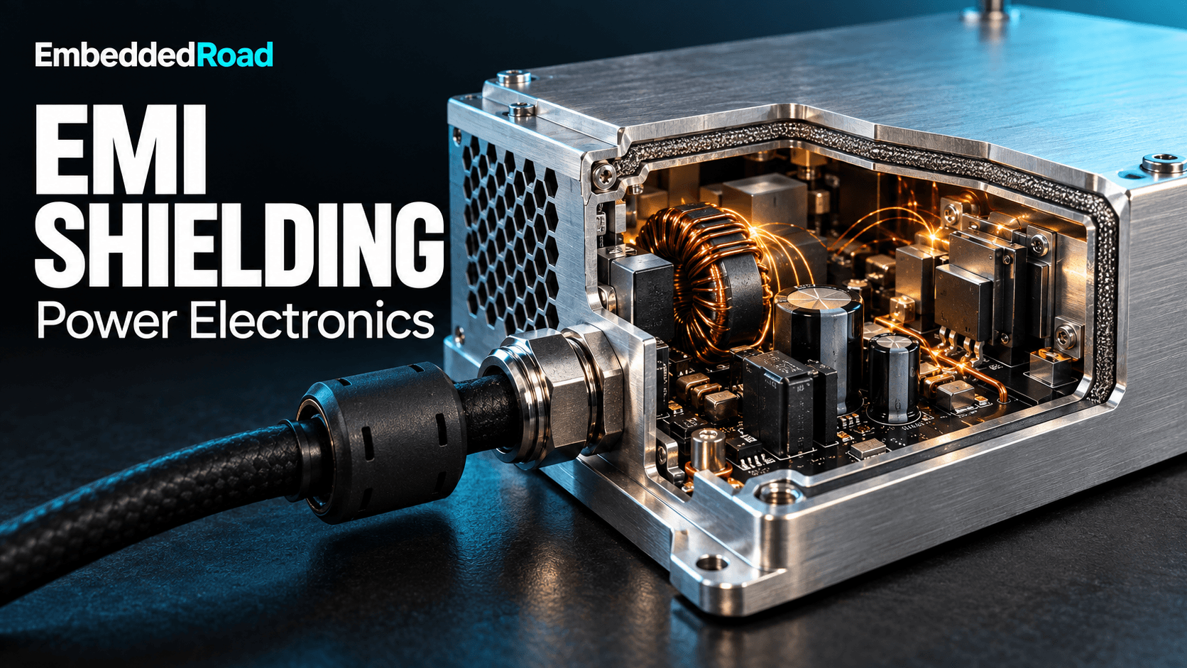
A fully welded metal enclosure gives the best SE but traps heat, adds cost and mass, and complicates serviceability. Design choices trade along three axes: SE (continuous metal > perforated mesh > plastic with conductive coating), cost (machined aluminum > die-cast > sheet metal > conductive paint), and thermal path (solid wall blocks convection; must add conduction path to an external heatsink or fans through filtered, EMI-rated vents). A common compromise is a perforated honeycomb vent, where hole diameter is kept below roughly λ/20 of the highest frequency of concern, trading some SE at the vent for substantial airflow.
Ferrite Bead: Absorption and Impedance Control
Frequency-dependent permeability and loss mechanism
A ferrite bead is not a simple inductor; its complex permeability µ = µ' – jµ'' means impedance has both reactive (µ') and resistive (µ'', loss) components, and above a cutoff frequency the resistive term dominates—the bead converts high-frequency noise current into heat within the ferrite rather than reflecting it back onto the line. This is why beads are effective broadband absorbers where a discrete LC filter would need multiple resonant stages. The impedance curve (R and X vs. frequency) in the manufacturer's datasheet is the only reliable source for this—do not assume a flat inductance value above a few MHz.
Placement on power, signal, and return paths
For maximum effect, a ferrite bead belongs in the current path closest to the noise source, before the noise has a chance to couple onto other traces: directly in series with a switching IC's power pin, or around a cable bundle right at the connector exit. A bead on a signal line does nothing if the return current path isn't also controlled—common-mode current ignores a bead placed on only one conductor of a differential pair unless it encircles both (a common-mode choke configuration). On power rails, bead placement upstream of the bulk decoupling capacitor, not downstream, keeps the LC combination from creating an unwanted resonance peak that amplifies noise at the resonant frequency instead of attenuating it.
Thermal effects and derating in high-current applications
Ferrite material saturates with DC bias, reducing µ' and the achievable impedance exactly when you need it most—high-current rails are the worst case. Manufacturers specify an impedance-vs-DC-bias curve; a bead rated 600 Ω at 100 MHz with zero bias might deliver a fraction of that at full load current. The resistive loss component also means real power dissipation in the bead itself (I²R in the lossy ferrite), which must be included in a thermal budget—verify with CFD thermal simulation (Ansys Icepak, FloTherm XT) when beads sit in an enclosed, low-airflow shielded compartment, since the shielding itself can trap the heat the bead generates.
Slot Antenna and Unintended Radiators
Gap and slot resonance in enclosures and connectors
A slot in a conductive surface radiates efficiently when its longest dimension approaches a half-wavelength of the exciting frequency (quarter-wave for a slot against a ground reference). A 15 cm seam gap resonates near 1 GHz; a 3 cm connector cutout gap resonates near 5 GHz. Unlike a wire antenna driven by current, a slot is driven by the voltage difference across it—induced by eddy currents in the shield wanting to flow across the gap—so even a shield with excellent material SE can radiate strongly if seams aren't continuous.
Identifying and sealing slot antenna modes
Near-field probing with a small loop antenna and spectrum analyzer, swept along seams and cutouts while the supply runs at full load, usually pinpoints the leaking aperture—look for field strength spikes localized to within a few millimeters of a specific gap rather than distributed evenly. Mitigation is mechanical: conductive gasket compressed to the manufacturer's specified deflection, overlapping (not butt-jointed) panel edges, and multiple grounding fingers rather than relying on a single screw per seam.
Cable routing and filtering at apertures
Any cable penetrating the enclosure is itself a potential slot-antenna feed if its shield isn't bonded to the enclosure wall at the point of entry. A cable shield grounded only at the far end, or through a short pigtail, lets common-mode current ride the cable outside the Faraday cage entirely—this is the single most common root cause of a radiated-emissions failure that appears only once cables are attached. Feedthrough filters or a ferrite clamp placed immediately at the aperture, combined with 360° shield bonding, close this path.
Multi-Layer Integration Strategy
Combining Faraday cages with ferrite filtering
Shielding and filtering solve different halves of the problem: the cage contains radiated fields; ferrite absorption and the common-mode EMI filter L-C, Pi, T topology reduce the conducted current that would otherwise excite the enclosure as an antenna in the first place. Treating them separately, bench-testing each stage's contribution with the other temporarily defeated (shield removed, filter bypassed), tells you which stage is actually limiting your margin instead of guessing.
Board-level shielding cans and compartmentalization
For mixed-signal boards (switching regulator next to an RF front-end or sensitive ADC), a stamped metal can soldered to a ground-stitched PCB perimeter creates a localized Faraday cage around the noisy section. Effectiveness depends on solder-joint continuity around the entire perimeter—gaps for component clearance reintroduce slot leakage at board level exactly as at enclosure level.
Return path integrity and via stitching
A shield or can is only as good as its ground reference. Via stitching at roughly λ/20 spacing around a shield's perimeter and along split-plane boundaries keeps return current on a short, predictable path rather than forcing it to detour around a plane discontinuity, which itself would create a radiating loop independent of the shield.
Measurement and Validation
Shielding effectiveness metrics and test setups
SE is measured per MIL-STD-285 or IEEE 299 style setups (transmit antenna, receiver, with and without the shield in place) for enclosures, or via a dedicated SE test fixture for gasket/material samples. For a full product, a pre-compliance radiated scan in a semi-anechoic chamber or a GTEM cell gives a faster, cheaper approximation before a formal accredited-lab run.
Common-mode filter verification post-shielding
After adding shielding, re-verify the conducted common-mode filter's performance with a LISN and spectrum analyzer rather than assuming the two stages are independent—a shield that changes parasitic capacitance to chassis can shift the common-mode filter's effective corner frequency.
Iterative design refinement for compliance margins
Treat the 6 dB (or greater, per your internal policy) margin below the regulatory limit as the design target, not the limit itself—production spread, cable variations, and test-site uncertainty routinely consume several dB. Iterate: near-field probe, identify dominant radiator, apply targeted fix (seam gasket, bead, filter retune), re-scan.
Thermal and Mechanical Constraints
Heat dissipation through shielded enclosures
A sealed metal enclosure that solves EMI can create a thermal problem by eliminating convective airflow. Options are a conductive path to an external heatsink, EMI-filtered vents with hole size below the aperture resonance limit, or liquid cooling for the highest-power designs. Model airflow and hot-spot temperature with CFD thermal simulation (Ansys Icepak, FloTherm XT) before committing to a sealed design, since a retrofit vent after EMC testing often reopens the slot-antenna problem you just closed.
Mechanical robustness and vibration isolation
Gasket material must maintain compression over the product's vibration and thermal-cycling life; a gasket that relaxes after a few hundred thermal cycles silently degrades SE without any visible failure. Specify gasket deflection and compression-set ratings from the manufacturer's data, not just initial SE numbers.
Component accessibility for serviceability
Every access panel, test point, and field-serviceable connector is a planned aperture—design its gasketing and grounding fingers as part of the original shield, not as an afterthought bolted on after the enclosure drawing is frozen, since retrofitted access panels are where production SE variance is worst.
Learning
Sign in to track your progress.
Evidence
Public projects engineers linked to EMI Shielding: Faraday Cage, Ferrite Bead, Slot Antenna.
No engineer has linked a project to this topic yet. Built something that proves it? Add the project and tag it with power-electronics-emi-shielding-faraday-cage-ferrite-bead-slot-anten — it then shows here and on your public profile.