
Shift Register: Serial-In Serial-Out (SISO), SIPO, PISO, PIPO
Shift register architectures explained: SISO, SIPO, PISO, and PIPO, with data flow, timing, control signals, and when to use each design.
Contents & prerequisites
What is a Shift Register?
Definition and Core Function
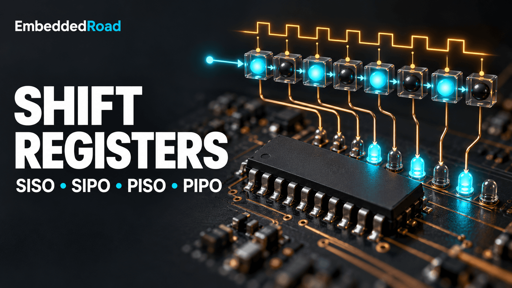
A shift register is a group of flip-flops connected in series or parallel, sharing a common clock, such that data moves one bit position per clock edge. Each flip-flop stores one bit, and the output of one stage typically feeds the input of the next. The "shift" in the name describes exactly what happens: on every active clock edge, the entire contents of the register slide over by one position, with a new bit entering at one end and the bit at the other end falling off (or being captured as output).
The building block is almost always a D flip-flop — for the underlying timing behavior of that cell, see D Flip-Flop: Rising-Edge Triggered, Timing Parameters. A shift register is nothing more than N of these flip-flops chained together with control logic around them to decide what gets loaded and where.
Role in Sequential Logic Circuits
Unlike combinational logic, which produces an output purely as a function of present inputs, a shift register has memory — its output depends on the history of what was clocked in. This makes it a sequential circuit by definition, and it's one of the first non-trivial sequential building blocks every digital designer learns after the flip-flop itself. It sits at the boundary between pure storage (a plain register) and data movement (a bus), because it does both at once.
Why Shift Registers Matter in Digital Design
Shift registers solve a problem that shows up constantly in embedded systems: converting between serial and parallel representations of data. Microcontroller pins are expensive; serial buses are cheap on pins but slow per bit; internal datapaths are wide and parallel. Shift registers are the glue that lets you trade pin count for time, or time for pin count, in a controlled, predictable way. They also underlie UARTs, SPI peripherals, LED drivers, and bit-serial arithmetic units.
Serial-In Serial-Out (SISO)
Architecture and Data Flow
A SISO register is the simplest case: a chain of D flip-flops where data enters serially at the first stage and exits serially from the last stage, with no other access points. Each stage's Q output connects to the next stage's D input, and all flip-flops share a common clock and (usually) a common reset.
Timing Diagram and Operation
On each rising clock edge, stage 1 captures the serial input bit, stage 2 captures what stage 1 held previously, and so on down the chain. An N-stage SISO register imposes exactly N clock cycles of latency between a bit entering and that same bit appearing at the output. If you inject a single '1' into an otherwise all-zero 4-stage register, you'll see that '1' walk out the far end exactly 4 clock edges later — a textbook way to verify wiring on a bench.
Practical Applications (delay lines, bit-serial processing)
SISO registers are used primarily as digital delay lines — deterministic, clock-cycle-accurate delays for synchronizing signals that arrive at different times, or for implementing FIR filter taps in bit-serial DSP architectures. Because there's no parallel access, they're cheap in gate count and routing but limited in utility outside of pure delay or serial pipeline applications.
Advantages and Limitations
Advantages: minimal pin count (just serial in, serial out, clock), simple control (no mode signals needed), low area. Limitation: you cannot observe or load the internal state except by shifting data all the way through, which makes SISO unsuitable whenever you need to inspect or set multiple bits at once.
Serial-In Parallel-Out (SIPO)
Architecture and Parallel Output Tap Points
A SIPO register is structurally identical to a SISO chain — same flip-flops, same serial-in connection — except every stage's Q output is also brought out to a dedicated pin or internal bus tap. This is the key architectural difference between SISO and SIPO: SISO exposes only the final bit, while SIPO exposes the state of every stage simultaneously.
Converting Serial Streams to Parallel Data
Data still enters one bit per clock edge, but after N clock cycles, all N bits are simultaneously available at the N parallel outputs. This is the canonical serial-to-parallel converter.
Timing and Clock Requirements
The parallel outputs are valid continuously (they reflect the current flip-flop state at all times), but they only represent a complete, meaningful word once exactly N clock edges have occurred since the start of a frame. Downstream logic needs a frame or "load complete" signal — often generated by a separate counter — to know when to latch the parallel bus rather than reading it mid-shift.
Real-World Use Cases (UART reception, protocol conversion)
This is exactly the mechanism inside a UART receiver: bits arrive serially at the baud rate, get shifted into an 8- or 9-bit SIPO register, and once a full frame has arrived, the parallel value is latched into a holding register readable by the CPU bus in a single access. SIPO ICs are also the standard way to drive parallel LED or relay banks from a microcontroller using only two or three pins (serial data, clock, and a latch-enable).
Parallel-In Serial-Out (PISO)
Architecture and Load/Shift Control
A PISO register has a D input at every stage, not just the first, plus a multiplexer in front of each flip-flop that selects between the parallel input bit and the shifted value from the previous stage. A single control line — commonly called LOAD/SHIFT or SH/LD̄ — switches every stage's multiplexer simultaneously.
Multiplexing Parallel Inputs onto Serial Line
When LOAD is asserted, the next clock edge captures the entire parallel word into the register in one cycle, each flip-flop taking its own corresponding parallel bit. When SHIFT is asserted instead, the mux routes the previous stage's Q into the current stage's D, and the register behaves exactly like a SISO chain, with the last stage's output serving as the serial output pin. This is how a PISO register converts parallel data into a serial stream: one parallel load cycle, followed by N shift cycles to stream the bits out one at a time, most-significant or least-significant bit first depending on wiring.
Control Logic and Mode Selection
The mode-select line must be set up before the relevant clock edge with adequate margin relative to the flip-flops' setup time, exactly as described for a single D flip-flop in the timing-parameters discussion linked above — a PISO register is just N such flip-flops whose setup-time requirement now applies collectively to the mux-select signal as well as to each data input.
Applications in Data Transmission (UART transmission, parallel-to-serial)
PISO is the mirror image of SIPO and is exactly what a UART transmitter does internally: the CPU writes a parallel byte into the shift register in one bus cycle, the hardware asserts LOAD, and then on each subsequent baud-rate clock tick it shifts one bit out onto TX. PISO registers are also the basis of input shift registers used to read many parallel switch or sensor lines into a microcontroller using few pins.
Parallel-In Parallel-Out (PIPO)
Architecture: Direct Parallel Path
A PIPO register has parallel inputs and parallel outputs at every stage with no serial connections required between adjacent flip-flops at all — though many real PIPO ICs also support shifting as a secondary mode, blurring the line with PISO/SIPO designs.
Register File Behavior and Data Routing
In its purest form, a PIPO block is just N D flip-flops clocked together, each independently capturing and holding one bit of a word — functionally a general-purpose register rather than a "shifting" structure at all. Data goes in all at once and comes out all at once, on the same clock edge.
Shift and Parallel Load Modes
Many commercial "universal" shift register parts (check the specific datasheet for exact mode-control truth tables) implement all four behaviors in one chip, selectable via two mode pins: parallel load, shift left, shift right, and hold. This is the general-purpose workhorse part designers reach for when the application might need any of SISO, SIPO, PISO, or PIPO behavior depending on firmware configuration.
Use in CPU Register Banks and Temporary Storage
PIPO structures are the direct ancestor of CPU register files and pipeline latches — any place where a whole word must be captured and made available in a single clock cycle, with no serial bottleneck. When a shift capability is added on top, the same hardware can also feed a barrel shifter for single-cycle arbitrary-amount shifts, which is the combinational complement to the one-bit-per-cycle shifting covered here.
Design Considerations and Timing
Propagation Delay Through Cascaded Stages
Each stage adds its clock-to-Q propagation delay before the next stage can act on the new data. In a synchronous design all stages are clocked together, so this delay doesn't accumulate across the chain the way it would in a ripple structure — but it does set a lower bound on the clock period: the clock-to-Q delay of one stage plus the setup time of the next must fit within one clock cycle, minus any routing delay.
Setup and Hold Time Constraints
Every stage boundary in a shift register is a separate timing path that must satisfy setup and hold constraints independently. With long chains (16, 32, 64+ stages), hold-time violations are the more insidious failure mode: if clock skew between adjacent flip-flops is large enough, a fast flip-flop can capture the new value of its neighbor instead of the old one, silently corrupting the shift. This is the same setup/hold mechanism covered for a single D flip-flop, just replicated at every stage boundary.
Clock Distribution in Multi-Stage Shifts
For long registers or high clock rates, clock skew across the chain becomes the dominant risk. If the clock arrives at stage 10 meaningfully later than at stage 9, the hold-time margin at that boundary shrinks or disappears. This is why wide shift registers in ASICs and FPGAs rely on balanced clock trees rather than daisy-chained clock buffers — an unbalanced clock net is a common root cause of "it works at low frequency but fails above X MHz" bugs.
Power Consumption in Sequential Shifting
Every clock edge toggles every flip-flop's internal nodes whether or not the data actually changes, so a continuously shifting register burns dynamic power proportional to clock frequency times stage count, regardless of data activity. Gating the clock during idle periods (common in SPI/UART peripherals between frames) is the standard mitigation.
Comparison Table and Selection Guide
SISO vs. SIPO vs. PISO vs. PIPO: Trade-offs
| Type | Input | Output | Typical Pin Count | Access to Intermediate Bits |
|---|---|---|---|---|
| SISO | Serial | Serial | Lowest | None |
| SIPO | Serial | Parallel | Moderate (N output pins) | Full, continuously |
| PISO | Parallel | Serial | Moderate (N input pins) | Only at load time |
| PIPO | Parallel | Parallel | Highest | Full, every cycle |
I/O Pin Count and Area Trade-offs
SISO and PIPO sit at opposite extremes of pin economy: SISO uses the fewest pins but gives the least visibility into the data; PIPO uses the most pins but gives full simultaneous access. SIPO and PISO are the practical compromise chips you'll actually buy — they trade a few extra pins (N parallel lines on one side) for a serial interface on the other, which is precisely the point of using them next to a microcontroller with limited GPIO.
Speed vs. Parallelism
Serial interfaces are slow per bit but pin-cheap; parallel interfaces are fast (one clock per word) but pin-expensive. A SIPO or PISO register is a deliberate point on that trade-off curve: it lets a serial link run at whatever bit rate the medium supports while presenting a full parallel word to the rest of the system once per frame.
When to Use Each Type
For a serial-to-parallel data converter — reading a serial sensor stream or a UART-like link into a byte-wide bus — use SIPO. For the reverse, sending a parallel register's contents out over a single wire, use PISO. Reach for SISO only when you need a pure, fixed-length delay line with no need to inspect intermediate state. Use PIPO (or a universal shift register configured for parallel load/output) when you need a general-purpose storage element that must present or accept a full word in a single clock cycle, such as a pipeline stage or a small register file.
Learning
Sign in to track your progress.
Evidence
Public projects engineers linked to Shift Register: Serial-In Serial-Out (SISO), SIPO, PISO, PIPO.
No engineer has linked a project to this topic yet. Built something that proves it? Add the project and tag it with digital-electronics-shift-register-serial-in-serial-out-siso-sipo-piso — it then shows here and on your public profile.