
BGA Breakout: Dog-Bone, Via-in-Pad Techniques
BGA breakout explained: dog-bone vs via-in-pad geometry, stub resonance, fill specs, and how to mix both methods by signal type.
Contents & prerequisites
Prerequisites
Why BGA Breakout Matters
The pitch-to-trace challenge
A 0.8 mm pitch BGA gives you roughly 0.4 mm of center-to-center spacing to work with between ball pads, and by the time you subtract pad diameter (typically 0.4 mm for a 0.8 mm pitch part) there's often less than 0.1-0.2 mm of copper-to-copper clearance left for a trace to pass through. Drop to 0.5 mm pitch — common on modern SoCs and FPGAs — and that gap shrinks below what most fabricators can reliably etch at standard tolerances. The breakout problem is purely geometric: you have N balls on a grid and you need N traces to escape that grid without shorting to a neighbor, and the pitch dictates how aggressively you need to route under the package rather than beside it.
Signal integrity and layer planning
Breakout isn't just a routing puzzle — it's where your stackup gets tested. Every signal that escapes a BGA transitions from a pad, through some combination of trace and via, onto a routing layer, and that transition is where impedance discontinuities, stub resonances, and crosstalk get baked in before the signal ever reaches "real" routing. Decisions made at breakout — which layer a differential pair escapes on, how far a via stub extends, how close two escape traces run — determine whether your eye diagram closes cleanly ten centimeters later. Treating breakout as an afterthought you'll "clean up in SI simulation" is a common and expensive mistake.
Manufacturing feasibility constraints
Your fabricator's minimum trace width/spacing, minimum drill size, and minimum annular ring all interact with ball pitch to determine which breakout strategies are even legal. A fab that quotes 3 mil/3 mil (0.075 mm) trace/space can dog-bone a 0.65 mm pitch BGA on two layers; the same fab may require via-in-pad to escape a 0.4 mm pitch part at all. Always pull your fab's current capability table before committing to a breakout strategy — don't assume last year's numbers still apply.
Dog-Bone Routing Fundamentals
Geometry and nomenclature (stub, neck, pad)
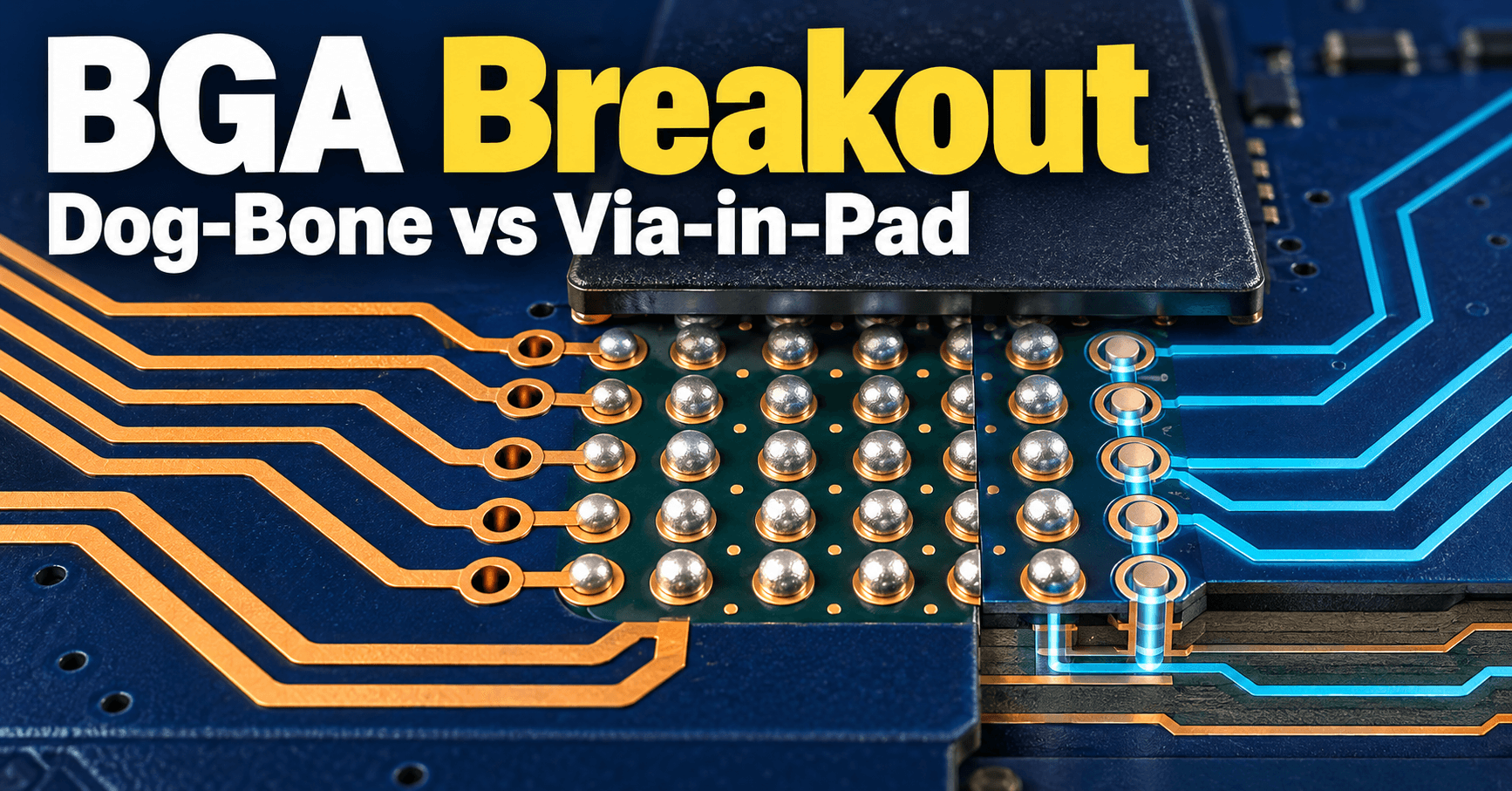
A dog-bone breakout places a via just outside the BGA pad, connected by a short trace called the neck, with the via itself sitting off-grid between four balls. The via's own pad, and the short unused length of trace or via barrel beyond the connection point, form the "stub" — electrically a tiny length of unterminated transmission line hanging off the signal path. The name comes from the shape: ball pad, narrow neck, via pad, resembling a dog bone in silhouette.
Trace width and spacing from adjacent balls
The neck trace typically runs 3-4 mil wide on fine-pitch parts, constrained by the diagonal clearance between four adjacent ball pads. For a 0.8 mm pitch BGA with 0.4 mm pads, the diagonal gap between pads is about 0.73 mm, enough for a single trace plus two spacings at most process nodes. At 0.5 mm pitch with proportionally sized pads, that diagonal gap can drop below 0.3 mm, forcing you either to thinner traces than your fab recommends or to a different escape method entirely. This is where the 3W rule for traces becomes hard to honor in the breakout region — you often can't maintain 3x trace width spacing between adjacent escape necks, which is exactly why crosstalk screening matters more here than anywhere else on the board.
When dog-bone is preferred over other methods
Dog-bone wins when pitch is generous enough (typically ≥0.8 mm) to route a trace between balls, when the signal is low-to-medium speed, and when you want to keep via count down and inspection straightforward — the via sits in open field, fully visible to AOI and X-ray, not hidden under a solder ball. It's also the default for cost-sensitive boards: no via-in-pad plating or plugging fees apply.
Stub length impact on stub resonance
The neck-plus-via-pad stub is a classic open-circuit transmission line stub, and it resonates at frequencies where the stub length approaches a quarter wavelength. A stub of length ℓ behaves as a notch filter with first resonance at f = v/(4ℓ), where v is the propagation velocity in your dielectric (roughly 1.5×10^8 m/s for FR-4 stripline). A 1.5 mm stub resonates near 25 GHz — fine for most digital signals — but a sloppy 5 mm stub drops that resonance to roughly 7.5 GHz, well within the harmonic content of a 2.5-3.2 Gbps serial link. For anything above a few hundred Mbps, measure your actual stub length from the pad edge to the via's farthest copper and check it against your target bandwidth's quarter-wave frequency before committing to dog-bone.
Via-in-Pad Technique and Implementation
Solder-filled vs. plugged via definitions
Via-in-pad places the via directly inside the BGA land, eliminating the neck and its stub entirely. Because an open via under a solder ball would wick solder away from the joint and starve it, the via must be filled: either with conductive or non-conductive epoxy and capped with plating (per IPC-4761 Type VII), or with solder paste reflowed to fill the barrel before the BGA is placed (less common, less reliable for larger drills). "Plugged" generally refers to the epoxy-fill-and-cap process; "solder-filled" is sometimes used loosely but risks voiding if the barrel isn't fully wetted.
Via diameter and escape routing layers
Via-in-pad holes are typically laser-drilled microvias, 0.075-0.15 mm finished diameter for HDI builds, small enough to fit entirely within a 0.3-0.4 mm BGA pad with annular ring to spare. Because the via sits under the ball, the escape trace connects to the via's lower end on an inner or bottom layer, meaning your layer stackup must provide a routing layer immediately beneath the via termination — this is where stackup planning and breakout planning become the same exercise.
Thermal performance and via stitching patterns
Via-in-pad is the standard technique for thermal and power balls: an array of filled vias directly under a ground or power pad conducts heat to an internal plane far more effectively than a dog-boned trace ever could. For thermal pads under QFN-style center pads or power BGAs, a grid of 0.3 mm filled vias on 1 mm centers is a common starting point, refined against your thermal simulation.
Reliability: IPC-2222 and assembly risk factors
IPC-2222 and IPC-6012 class requirements govern annular ring and plating thickness for filled vias, but the practical risk is incomplete fill: a void in the epoxy plug can trap flux volatiles, which expand during reflow and push the via cap outward, cracking the solder joint above it (a "popcorning" failure). Specify fill class and require your fab to report void content via microsection or X-ray on first article boards.
Hybrid Breakout: Combining Both Methods
Ball assignment strategy by signal type
Most real designs mix both techniques ball-by-ball. A practical rule: route power, ground, and low-speed GPIO with dog-bone (cheap, inspectable), and reserve via-in-pad for high-speed differential pairs, thermal pads, and any ball where the neighboring pitch is too tight for a legal dog-bone neck.
High-speed signals: when to use dog-bone vs. via-in-pad
For signals above roughly 1 Gbps per lane, favor via-in-pad to eliminate stub resonance entirely — there's no neck, so there's effectively zero open-stub length. If dog-bone must be used for a high-speed net (common on lower-layer-count boards), consider back-drilling or using blind/buried vias to shorten the resonant stub, and recheck with the same quarter-wave math from the dog-bone section.
Power and ground ball handling
Power and ground balls benefit from via-in-pad regardless of speed, since the goal there is low inductance and good thermal conduction, not signal fidelity — a short dog-bone neck adds unwanted series inductance to a power delivery path that's trying to look like a low-impedance plane connection.
Design rule automation in layout tools
Modern PCB tools let you define breakout rules per net class — assign "via-in-pad, 0.1 mm microvia" to a diff-pair net class and "dog-bone, 4 mil neck" to a GPIO class, then let the autorouter or interactive router apply them automatically during fan-out. Set these rules before you start placing escape vias; retrofitting mixed breakout after manual fan-out is tedious and error-prone.
Layout Best Practices and Tradeoffs
Via-in-pad cost and turnaround impact
Via-in-pad adds a fill-and-cap-plate process step that most fabs quote as a per-panel adder and an extended turnaround (often +2-5 days versus standard through-hole vias). For a board with hundreds of filled vias, this can meaningfully shift unit cost and prototype lead time — budget for it early rather than discovering it at quote time.
Acid trap risk and plugged via specifications
Dog-bone necks that meet via pads at acute angles create acid traps — pockets where etchant or plating solution pools and over-etches the copper, thinning the neck. Keep neck-to-pad junctions at 90° or greater, and route necks straight into the via center rather than at a tangent. For plugged vias, specify fill material, void limit (percentage by volume, commonly ≤5%), and cap plating thickness explicitly in fab notes — "standard via fill" without numbers invites inconsistent results across vendors.
Trace length matching for clock and data nets
Breakout geometry changes effective trace length per pin, which matters for length-matched buses. A dog-boned pin gains neck length plus some via barrel; a via-in-pad pin effectively starts its length budget at the ball. When matching a DDR byte lane or a clock-to-data skew budget, include breakout stub/neck length in your length calculations, not just the "obvious" routed trace on the main layer.
Layer stackup interaction with BGA escape
The number of layers available directly under the BGA footprint — before signals can fan out to full board routing — determines how many balls you can escape per layer and whether you need blind/buried vias at all. A 4-layer stackup escaping a 676-ball, 1 mm pitch BGA will struggle; the same device on an 8-layer or HDI stackup with via-in-pad has room to breathe. Review your microstrip controlled impedance formula target early, because the dielectric thickness needed for 50 Ω or 100 Ω differential routing on inner layers constrains how thin (and therefore how breakout-friendly) those layers can be.
Signal Integrity and Design Verification
Stub resonance and reflection management
Simulate the dog-bone stub as a short transmission line stub in your SI tool (most field solvers and SPICE-based channel simulators support this directly) rather than ignoring it as "just a via." Confirm the stub's quarter-wave resonance sits comfortably above your signal's Nyquist frequency plus margin — a common target is 2-3x headroom.
Controlled impedance routing from breakout to bulk
The transition from ball pad through neck/via into bulk trace routing is a local impedance discontinuity even when both ends are nominally 50 Ω or 100 Ω differential, because pad capacitance and via barrel inductance don't match trace geometry. Keep the discontinuity short and symmetric (especially for diff pairs — route both legs through matched breakout geometry) and verify with TDR simulation or measurement on first silicon.
Eye diagram simulation with escape topology
For serial links above a few Gbps, include the actual breakout topology — stub length, via barrel, pad capacitance — in your channel model, not an idealized trace. An eye diagram run without breakout parasitics will look better than silicon ever will; the gap between the two is exactly the stub and pad effects discussed above.
Crosstalk between adjacent escape traces
Escape regions pack traces closer together than anywhere else on the board, making them the highest-crosstalk zone by construction. Where you can't hold 3W spacing, compensate with ground stitching vias between escape traces or by routing sensitive pairs on different layers through the breakout zone, then reconverge once traces reach open routing channels.
Fabrication and Assembly Considerations
Netlist and layer stackup coordination
Confirm with your fab that the netlist-driven DFM check accounts for via-in-pad fill requirements per layer — a via specified as "filled" on an inner layer but left open on an outer layer due to a stackup miscommunication is a common first-article defect.
Solder mask clearance and paste mask vias
Via-in-pad pads need solder mask defined correctly so the cap plating, not raw copper, is exposed at the surface, and paste mask apertures must match the capped pad exactly — oversized paste apertures over a filled via can cause solder beading or insufficient wetting.
X-ray inspection points for via fill quality
Request X-ray inspection of a sample of filled vias per panel, focusing on void content and cap plating continuity; this is the only non-destructive way to catch a fill defect before it becomes a field failure under thermal cycling. Pair this with your copper balancing and hatching plan review, since uneven copper distribution around dense via-in-pad arrays can locally distort CTE and stress the very joints you're trying to protect.
Component rework and replaceability limits
Via-in-pad boards are harder to rework than dog-bone boards: reflowing a BGA with filled vias under every ball risks disturbing the plug/cap interface on repeated heat cycles, and there's no accessible via to probe for in-circuit test. If your product requires field rework or extensive ICT, weigh that against the SI gains of via-in-pad before applying it board-wide.
Learning
Sign in to track your progress.
Evidence
Public projects engineers linked to BGA Breakout: Dog-Bone, Via-in-Pad Techniques.
No engineer has linked a project to this topic yet. Built something that proves it? Add the project and tag it with hardware-hw-bga-breakout-dog-bone-via-in-pad-techniques — it then shows here and on your public profile.