
Creepage and Clearance: Function of Working Voltage and Pollution Degree
Creepage and clearance explained for medical device PCBs: how working voltage and pollution degree set exact IEC 60601-1 spacing values.
Contents & prerequisites
Why creepage and clearance matter in medical device safety
Creepage distance is the shortest path between two conductive parts measured along the surface of an insulating material; clearance is the shortest path between the same two parts measured straight through air. The distinction matters because the two paths fail by different mechanisms and are governed by different physics — a PCB can have ample clearance (air gap) between a mains-referenced trace and a patient-connected trace while still having a creepage path short enough to carbonize and flash over in humid conditions. IEC 60601-1 (the base safety standard for medical electrical equipment) treats them as independent parameters, and a design has to satisfy both minimums simultaneously, not whichever is larger.
Electrical insulation failure modes in clinical environments
Surface tracking is the dominant creepage failure mode: moisture, saline aerosol, or conductive dust bridges the gap, a leakage current flows, and localized heating carbonizes the substrate until a permanent conductive track forms. Clearance failures look different — they are dielectric breakdown events, where an air gap that was adequate at sea level and 20 °C arcs over under a transient overvoltage, high altitude (lower air density), or elevated temperature. A device that spends its life in an operating room sees alcohol-based disinfectant wiped across enclosure seams and connector shrouds, which is a far more aggressive creepage stressor than the clean, low-humidity benchtop environment where the prototype was first bench-tested.
Role in IEC 60601 compliance and risk management
IEC 60601-1 treats creepage and clearance as a primary means of protection against electric shock, alongside protective earthing and double insulation, and auditors check these dimensions directly against the standard's tables rather than accepting a qualitative "looks fine" assessment. Because insulation is a basic safety function, undersized spacing is classified as a hazard in the risk management file (per ISO 14971), not a mere nonconformance — it has to be tracked, mitigated, and verified with documented measurements, not just redesigned and forgotten.
Consequences of undersized distances in patient-contact devices
A creepage or clearance violation on a patient-connected circuit can put mains-derived or line-frequency leakage current directly onto a patient-applied part, which is the exact failure mode IEC 60601-1's means-of-protection scheme exists to prevent. In practical terms this shows up as failed dielectric withstand (hipot) testing, failed leakage current measurements, or — worse — a field failure where insulation breakdown under disinfectant exposure energizes a housing or sensor lead that the patient or clinician touches.
How working voltage determines minimum creepage distance
Creepage distance scales with the working voltage because higher potential drives more leakage current through any surface contamination film and accelerates the tracking process. Working voltage, not supply voltage, is the number in the equation: it's the actual RMS or DC voltage that insulation sees in normal operation, including any DC bias superimposed on an AC waveform.
Voltage-dependent breakdown risk along PCB surfaces
Surface tracking is a cumulative, current-driven process, so the relationship between voltage and required creepage is not linear at low voltages but grows steeply above a few hundred volts, which is why the IEC 60601-1 tables jump distances in coarse voltage bands rather than a smooth formula.
Calculating creepage from rated working voltage and transient overvoltage
In practice you don't compute creepage from first principles — you determine two inputs and look up the result. First, find the working voltage RMS across the specific insulation barrier (e.g., mains-to-secondary, or secondary-to-patient-connection). Second, determine the pollution degree and material group for that location on the board. Then read the required distance from IEC 60601-1's Table 11 (basic insulation) or the corresponding reinforced-insulation column, cross-referenced against IEC 60664-1 for the underlying low-voltage creepage/clearance methodology that 60601-1 incorporates by reference. Transient overvoltage (from the mains overvoltage category) sets the clearance side of the calculation, not creepage, but both numbers come from the same voltage characterization exercise, so do them together.
Medical device voltage categories and their isolation requirements
A single device commonly has three or four distinct working voltages to characterize: the mains input (100–240 V AC), an isolated low-voltage secondary (often 5–24 V DC), and a patient-connected signal path that may be at only a few millivolts but still requires full means-of-patient-protection spacing because of what it's connected to, not what voltage it carries. A temperature sensor interface such as an NTC, RTD Pt100, or infrared thermopile front end is a good example: the sensor signal itself is tiny, but if the sensor contacts the patient, the isolation barrier between that circuit and any mains-referenced circuitry still has to meet full patient-protection creepage and clearance, sized by the mains working voltage on the other side of the barrier, not by the sensor signal.
How working voltage determines minimum clearance distance
Clearance is set by the dielectric strength of air and scales with both the working voltage and the expected transient (impulse) overvoltage, because air gaps fail by sudden breakdown rather than gradual tracking. The relevant number for sizing clearance is the peak voltage the gap must withstand, including mains transients, not the steady-state RMS value used for creepage.
Air gap insulation strength as a function of voltage
Dry air breaks down at roughly 3 kV/mm at sea level under uniform field conditions, but PCB geometries are rarely uniform-field, and altitude matters: air density drops with elevation, so a clearance adequate in a ground-floor clinic may be undersized for the same device shipped to a high-altitude facility. IEC 60601-1 handles this with altitude correction factors applied above 2000 m — check the applicable clause if the device is specified for high-altitude installations.
Safety factor application for clearance in medical circuits
Clearance tables already embed a safety margin for manufacturing tolerance and field non-uniformity, so designers should not "round down" to the table minimum when stack-up tolerances could consume the margin — a 0.1 mm PCB solder-mask registration error is not negligible on a 1.5 mm clearance requirement.
Spacing between high-potential and ground conductors
Clearance has to be measured as the shortest straight-line air path, which may run diagonally between a trace on the top layer and a via barrel, not just the horizontal spacing visible in the layout view — a common audit finding is adequate horizontal spacing undermined by a grounded mounting screw or heatsink positioned above the gap.
How pollution degree affects creepage and clearance tables
Pollution degree describes the expected contamination of the micro-environment immediately around the insulation, and it multiplies the required creepage distance independently of voltage. IEC 60664-1 defines four degrees, summarized here as applied in medical enclosures:
| Pollution Degree | Environment | Typical Medical Context |
|---|---|---|
| PD1 | No pollution, or only dry, non-conductive pollution | Hermetically sealed, potted assemblies |
| PD2 | Normally non-conductive pollution, occasional temporary condensation | Enclosed PCB inside a device housing (most common assumption) |
| PD3 | Conductive pollution, or dry non-conductive pollution expected to become conductive from condensation | Open PCB exposed to room air, unsealed enclosures |
| PD4 | Continuous conductivity from rain, snow, or conductive dust | Outdoor or heavily contaminated industrial settings (rare for medical) |
Pollution degree definitions (PD1–PD4) in medical environments
Most medical electrical equipment is assigned PD2 for internal PCB assemblies, on the assumption that the enclosure keeps out liquid ingress and dust but condensation is still plausible during transport or storage temperature swings. A board with conformal coating over the specific insulation gap can sometimes justify PD1 locally, but this has to be stated explicitly in the risk file and supported by the coating's qualification, not assumed.
Why higher pollution degree requires larger distances
Each step up in pollution degree increases the conductive-film probability on the insulation surface, so the tables compensate with larger required creepage — typically 1.5 to 2 times the PD2 value when moving to PD3 at the same voltage, though the exact multiplier depends on the specific voltage row, so read it from the table rather than approximating.
Real-world pollution in hospitals, clinics, and home care settings
For a portable medical device used in a hospital, PD2 is the standard default for internal electronics inside a closed enclosure; PD3 becomes the right assumption only for externally exposed contacts, battery compartments opened frequently by non-technical staff, or home-care devices that may sit in a bathroom or kitchen with condensation exposure. A device used for continuous intracranial pressure (ICP) monitoring in an ICU, for instance, typically keeps its signal-conditioning electronics in a sealed enclosure (PD2) while the external cabling to the sensor is evaluated separately for the bedside environment it actually sits in.
How to select creepage and clearance from IEC 60601-1 tables
The official tables live in IEC 60601-1 (clause 8.9 and its associated annexes) for the medical-specific values, built on the general methodology of IEC 60664-1; there is no substitute source, and a design history file (DHF) should cite the specific edition and amendment used, since minimum values have changed between editions.
Reading voltage and pollution degree cross-reference matrices
The tables are indexed by working voltage (in RMS or peak, read the column header carefully), pollution degree, and material group — find your voltage row, your pollution degree sub-column, and your material group sub-column, and the cell is the minimum distance in millimeters. A worked example: a secondary circuit with 60 V RMS working voltage, PD2 environment, and Material Group IIIa PCB substrate might require roughly 1.4 mm creepage per the applicable 60601-1 table row — but confirm the exact figure against the current edition table rather than this illustrative number, since the tables are revised and the actual value depends on the specific insulation type (basic vs. reinforced) being evaluated.
Reinforced vs. basic insulation requirements
Yes — reinforced insulation requires materially larger creepage and clearance than basic insulation at the same voltage and pollution degree, because reinforced insulation is defined as providing a degree of protection equivalent to double insulation using a single material system, with no accessible intermediate point. In practice, the reinforced-insulation column in the 60601-1 tables runs close to double the basic-insulation value at a given voltage and pollution degree, though not exactly 2x in every row — always read both columns rather than multiplying.
Derating for material group and comparative tracking index (CTI)
Material flammability and tracking resistance change the creepage requirement through the Comparative Tracking Index (CTI), a measured value (in volts) indicating how much voltage a material surface can withstand before tracking failure under standardized contamination testing. Materials are grouped — Material Group I (CTI ≥ 600), II (400–600), IIIa (175–400), IIIb (100–175) — and lower material groups require larger creepage at the same voltage and pollution degree because they're more prone to tracking. Standard FR-4 PCB laminate typically falls in Material Group IIIa, which is why most PCB creepage tables default to that column; if a vendor can document a higher CTI substrate, creepage can sometimes be reduced, but this requires a traceable material certificate in the DHF, not an assumption.
Practical layout rules for PCB designers on medical devices
Treat creepage and clearance as layout constraints to be enforced with design rule checks (DRC), not post-layout verification items, because retrofitting spacing into a routed board usually means a respin. Set the DRC minimum spacing rule for any net crossing a safety isolation barrier to the table value plus a manufacturing margin — many teams add 0.1–0.2 mm above the calculated minimum to absorb etching and registration tolerance.
Trace routing and spacing guidelines for high-voltage sections
Route the isolation barrier as a keep-out zone with no traces, vias, or copper pour crossing it except the intentional isolation components (opto-isolators, isolated DC-DC converters, isolation transformers), and verify the slot or routed gap width directly against the clearance table rather than the silkscreen outline, since copper pour relief and solder mask openings can quietly narrow the actual gap.
Component placement to minimize creepage paths
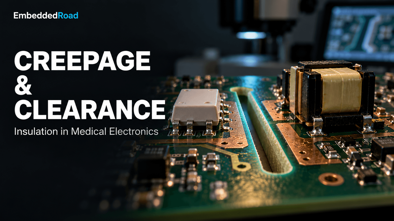
Avoid placing through-hole components with long exposed leads across an isolation barrier, since the lead itself becomes part of the creepage path measurement and often has a shorter surface distance than the PCB track layout suggests; slots cut through the PCB substrate between isolated sections are a standard technique to extend the effective creepage path without enlarging the board.
Conformal coating and physical barriers as auxiliary measures
Conformal coating can justify a reduced pollution degree assumption (moving an exposed PD3 location to an effectively PD2 evaluation) only when the coating process and material are qualified per IEC 60664-3, and this qualification — not just "we spray the board" — has to appear in the verification record.
Verification and documentation for design history file (DHF)
Every isolation barrier on the schematic should have a traceable entry in the DHF showing the working voltage used, pollution degree assigned, material group, the table and edition referenced, the resulting minimum distance, and a measured or layout-extracted actual distance confirming compliance — auditors routinely ask for this cross-reference during a technical file review.
When to apply enhanced margins and worst-case analysis
Apply margins beyond the table minimum whenever manufacturing tolerance, aging, or environmental stress could plausibly erode the as-designed distance below the regulatory floor during the product's service life. The table values are compliance minimums under specified test conditions, not a margin-inclusive engineering target.
Tolerance stack-up in manufacturing and aging
PCB fabrication tolerances (trace position, solder mask registration), connector seating variation, and enclosure assembly tolerance all subtract from the nominal designed spacing, so a worst-case stack-up calculation — not just the nominal CAD distance — should be checked against the table minimum, particularly for connector-based isolation barriers where mechanical tolerance dominates.
Environmental stress testing (humidity, temperature cycling)
Humidity cycling and thermal cycling can degrade conformal coating adhesion, open hairline cracks at solder joints near isolation barriers, or allow condensation to form in a sealed enclosure that was assumed to maintain PD2 — IEC 60601-1's environmental test sequence exercises exactly these failure paths, and spacing verification should be repeated after stress testing, not only on as-built units.
Risk assessment triggers for increased safety distances
Increase margins above table minimums when the risk analysis identifies a patient-connected circuit with no secondary protection, a device intended for home use with uncontrolled pollution exposure, or a reusable device subject to repeated disinfectant wiping that could degrade coating or housing seals over time — in each case, document the rationale for the added margin in the risk management file so the extra spacing reads as a deliberate mitigation, not an unexplained design choice.
Related reading
- Electrical Safety: Protective Earth, Leakage — relating board spacing to shock protection.
Learning
Sign in to track your progress.
Evidence
Public projects engineers linked to Creepage and Clearance: Function of Working Voltage and Pollution Degree.
No engineer has linked a project to this topic yet. Built something that proves it? Add the project and tag it with medical-devices-creepage-and-clearance-function-of-working-voltage — it then shows here and on your public profile.