
Isolation Barriers: Creepage, Clearance, Dielectric Strength
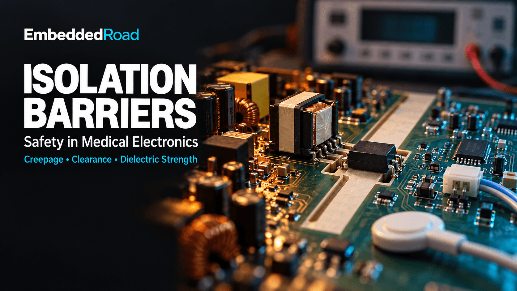
Learn to calculate creepage, clearance, and dielectric strength margins for medical device isolation barriers per IEC 60601-1.
Contents & prerequisites
Why isolation barriers matter in medical device safety
An isolation barrier is the physical and electrical separation between a patient-connected circuit and hazardous voltages — mains power, battery charging circuits, or any other energy source capable of delivering a harmful shock. In a medical device, that barrier is not a design nicety; it is the single feature standing between a patient with a conductive path through their body (an ECG lead, an invasive catheter, a dialysis line) and a fault current that would otherwise find the shortest route to ground through them.
Patient safety and regulatory requirements
IEC 60601-1 (the base safety standard for medical electrical equipment) treats isolation as a quantifiable, testable barrier property rather than a qualitative design goal. It defines means of patient protection (MOPP) and means of operator protection (MOOP), each requiring a specific combination of creepage distance, clearance, and dielectric withstand voltage depending on the working voltage and the degree of patient contact. A device with an applied part that touches the patient's skin needs at least two MOPP between that part and any hazardous voltage — meaning two independent barriers, each capable of containing a single fault, so that one failure does not leave the patient exposed.
Failure modes of inadequate isolation
Insufficient creepage or clearance does not fail gracefully. Surface contamination, humidity, or a solder bridge can turn a marginal gap into a conductive path over months of field use, long after the device passed its factory hipot test. The failure modes are leakage current exceeding IEC 60601-1 limits (microamp-level chronic exposure for cardiac-connected applied parts), carbonized tracking across a PCB that creates a permanent low-resistance path, or outright dielectric breakdown under a transient — a defibrillator discharge, an ESD event, or a mains surge — that punches through an air gap or insulation layer that looked adequate on paper.
Risk-based approach to barrier design
Barrier design should start from the risk management file, not from a spacing table. ISO 14971 requires that isolation failure be analyzed as a specific hazard with its own severity and probability estimate, and the creepage/clearance/dielectric strength values chosen should trace back to that analysis — not just to the minimum row in a standard's table. A device intended for use in a damp, dusty field environment should be designed to a tighter pollution degree assumption than the standard's default, because the standard's minimums assume the stated test conditions hold for the life of the device.
How creepage distance differs from clearance and why both matter
Creepage distance and clearance are both measured in millimeters between two conductive parts, but they protect against different failure physics and neither can substitute for the other.
Creepage: surface tracking and conductive paths
Creepage distance is the shortest path between two conductors measured along the surface of the insulating material between them. Failure here happens slowly: moisture, dust, and ionic contamination on a PCB or enclosure surface create a conductive film, and sustained voltage across that film causes localized heating and carbonization — tracking — that permanently lowers the surface resistance. Once a track forms, the effective creepage distance is gone and the path conducts at far lower voltages than the original clean surface would have allowed.
Clearance: air gaps and breakdown voltage
Clearance is the shortest distance through air between two conductors. Its failure mode is an instantaneous dielectric breakdown — ionization of the air gap under a high transient voltage — not a slow degradation. Clearance is primarily a function of peak voltage and altitude (air breakdown strength drops as atmospheric pressure drops), while creepage is a function of working voltage, pollution degree, and material group.
Pollution degree and environmental factors
Pollution degree describes the expected contamination of the micro-environment around the barrier, and it directly multiplies the required creepage distance. IEC 60601-1 defines four degrees: PD1 (no pollution, sealed/potted assemblies), PD2 (normal indoor environment, occasional condensation), PD3 (conductive pollution or dry non-conductive pollution that can become conductive from condensation), and PD4 (continuous conductivity from rain, snow, or conductive dust). Most mains-powered clinical equipment in an enclosed housing is designed to PD2; portable or point-of-care devices operating outside a controlled hospital environment are often pushed to PD3 by their intended-use environment, roughly doubling the required creepage distance for a given voltage compared to PD2.
Material group classification and selection
Material group classification is based on the comparative tracking index (CTI), a measured voltage at which a material under test surface-tracks to failure. IEC 60601-1 recognizes Material Group I (CTI ≥ 600 V), Group II (400 V ≤ CTI < 600 V), Group IIIa (175 V ≤ CTI < 400 V), and Group IIIb (100 V ≤ CTI < 175 V). A higher CTI material permits shorter creepage distances for the same voltage and pollution degree, which matters directly on space-constrained PCBs.
| Material Group | CTI Range | Typical Use |
|---|---|---|
| I | ≥600 V | High-reliability connectors, terminal blocks |
| II | 400–599 V | General PCB laminate, enclosure plastics |
| IIIa | 175–399 V | Cost-sensitive enclosures, lower pollution degree only |
| IIIb | 100–174 V | Generally avoided for reinforced isolation barriers |
How to calculate and verify creepage and clearance per IEC 60601-1
Required creepage and clearance values come out of lookup tables in IEC 60601-1 and its collateral IEC 60601-1-2, indexed by working voltage, pollution degree, material group, and isolation type — never off a single generic number.
Voltage rating and isolation type (functional vs. reinforced)
Functional isolation separates circuits for operation only and carries no patient-safety claim; basic isolation provides one layer of protection against electric shock; reinforced isolation is a single barrier equivalent to two basic barriers and is the usual choice for patient-connected circuits crossing a mains-derived supply. Reinforced isolation roughly doubles the creepage and clearance requirement of basic isolation at the same working voltage, and it must also pass a dielectric withstand test at a correspondingly higher voltage.
Creepage path measurement on PCB layout
On a PCB, creepage is measured along the board surface following every groove, slot, and edge, not as a straight line — a routed slot between isolated planes increases the effective creepage path without increasing board width, which is why slotting is the standard technique for meeting a 8 mm reinforced-isolation creepage requirement on a 4 mm-wide isolation zone. A worked check:
Required creepage (250 Vrms working voltage, reinforced,
PD2, Material Group II): 8.0 mm   [IEC 60601-1, Table 11]

Available straight-line board width across isolation gap: 5.0 mm
Slot width added: 1.0 mm, slot depth through full board thickness
Effective creepage path (board edge-to-edge around slot):
  5.0 mm (top surface, split by slot) -> path now routes down
  one slot wall, across the bottom, up the other wall
  = 5.0 mm (remaining surface) + 2 x 1.6 mm (board thickness, slot walls)
  = 8.2 mm  -> meets 8.0 mm requirement with 0.2 mm margin
Design margins and safety factors
A 0.2 mm margin on paper disappears the moment manufacturing tolerance, solder mask registration, or connector creep is added. Most medical device teams carry a 20–30% margin over the table minimum specifically to absorb PCB fabrication tolerance (typically ±0.1–0.15 mm on routed features), conformal coating creep, and the uncertainty in exactly where a connector pin's effective conductive edge sits.
Common mistakes in barrier routing
The recurring layout error is routing a ground-referenced shield, a test point, or a mounting hole pad through the isolation gap — any conductive feature, including an unused copper pour, counts as a conductor for creepage/clearance purposes even if it carries no signal. Silkscreen text and solder mask are not insulation for creepage calculations unless specifically qualified as such.
What dielectric strength testing reveals about barrier integrity
Dielectric withstand voltage (DWV) testing — often called a hipot test — applies a voltage well above working voltage across the barrier and confirms it does not break down, revealing latent defects that spacing measurements alone cannot catch, such as voids in potting, contamination trapped during assembly, or a hairline crack in insulation.
Dielectric withstand voltage (DWV) test methodology
The test applies either an AC voltage (typically 1 minute dwell) or a DC voltage (typically higher magnitude, shorter dwell) across the barrier and monitors leakage current; a sustained rise in leakage current or a current spike indicating arc-over is a fail. IEC 60601-1 specifies the exact test voltage as a function of the barrier's working voltage and isolation type — reinforced isolation barriers are tested at a higher voltage than basic isolation at the same working voltage.
Relationship to creepage, clearance, and material thickness
DWV testing and creepage/clearance design are complementary, not redundant: creepage and clearance tables are derived from long-term field statistics on tracking and breakdown, while the DWV test is a direct, per-unit or per-sample proof that this specific barrier, as built, holds off the specified voltage. Insulation thickness interacts with both — thin solid insulation can pass a DWV test while still failing to provide adequate long-term partial-discharge resistance, which is why solid insulation thickness has its own minimum requirement independent of the voltage withstand result.
Test conditions and dwell time
Test conditions matter as much as the voltage value: temperature, humidity, and dwell time are specified because dielectric strength of solid insulation and conformal coating degrades with temperature and prior humidity exposure. A barrier tested only at 25 °C, 1 minute dwell, on a dry bench sample does not represent a device that will see 80% relative humidity in clinical use.
Pass/fail criteria and documentation
Pass/fail is typically a hard leakage-current threshold plus absence of visible or audible breakdown (arcing, smoke, flashover); every unit tested in production should log the applied voltage, dwell time, and measured leakage current as objective evidence in the device history record, not just a binary pass stamp.
How material selection affects isolation performance
Insulation material grades and tracking indices
Material selection sets the achievable creepage distance for a given footprint: a Material Group I enclosure plastic or standoff lets a layout hold reinforced isolation clearance in a smaller area than a Group IIIa equivalent, which matters in handheld and wearable form factors where board area is the scarcest resource.
PCB laminate properties and layer spacing
Standard FR-4 laminate is generally Material Group II; its CTI and the resin system's moisture absorption both affect long-term creepage performance, especially when internal layer spacing (not just surface creepage) is used to implement an internal reinforced barrier between inner copper layers.
Component placement relative to isolation boundaries
Every component that straddles or sits near an isolation boundary — optocouplers, isolation transformers, Y-capacitors — has its own datasheet-specified creepage and clearance across its package, and the PCB layout must preserve that spacing on the board in addition to the component's internal isolation; a correctly rated optocoupler mounted with its pins bridged by a tight ground pour defeats its own isolation rating.
Coating and potting for environmental protection
Conformal coating and potting compounds can legitimately reduce the effective pollution degree seen by a barrier (moving a PD3 environment down to an effective PD2 assumption for the coated barrier), but only when the coating process and material are qualified and controlled — an uneven coat that leaves a thin uncoated gap at a connector pin provides a false sense of margin.
How to integrate isolation barriers into risk management and design controls
Failure mode analysis for isolation faults
Isolation faults belong in the device FMEA as a distinct failure mode — single-fault condition for both basic barriers in a reinforced pair — with traceable mitigations back to specific layout rules, component ratings, and test steps, not a generic "isolation maintained" risk control statement.
Verification and validation strategy
Verification combines physical creepage/clearance measurement on first-article boards (often with a microscope or calibrated gauge against the layout drawing), 100% production DWV testing, and periodic sample testing under environmental stress (humidity soak, thermal cycling) to catch degradation modes that a single bench test at time zero cannot.
Design review checklist for isolation
A design review for isolation should walk every barrier in the schematic and confirm: working voltage and isolation type assigned, pollution degree justified by intended-use environment, material group documented for every insulating surface in the path, PCB creepage path measured (not assumed) on the actual layout, and DWV test voltage specified in the test procedure before boards are built — reviewing these on paper is far cheaper than discovering a routing error after tooling is cut.
Manufacturing controls and incoming inspection
Incoming inspection should verify laminate material certificates match the qualified Material Group, and fabrication drawings should carry explicit creepage/clearance critical dimensions with tolerance callouts, not leave spacing to the fabricator's default design rules.
How isolation barriers interact with EMC and grounding strategy
Ground plane continuity across isolation boundaries
A split ground plane at an isolation barrier must stay split in every layer and every connector shield path; a single via or mounting screw that bridges primary and secondary ground references silently shorts the barrier regardless of how well the creepage and clearance were calculated.
ESD paths and patient-leakage current limits
An isolation barrier and an ESD protection strategy address related but distinct threats, and a device that handles electrostatic discharge events according to ESD Immunity: IEC 60601-1-2 Basic/Enhanced Performance still needs its creepage and clearance sized for sustained working voltage and transient withstand, since a discharge path engineered to protect electronics from an ESD event can itself become an unintended leakage path if routed across the patient isolation boundary.
Shielding integration with creepage/clearance spacing
Shield layers and chassis connections introduced for EMC compliance add conductive surfaces near the barrier, and each one needs its own creepage and clearance check to the isolated side — an EMC fix added late in development is a common source of isolation regressions that first-pass layout review would have caught.
Related reading
- Electrical Safety: Protective Earth, Leakage — grounding and leakage-current considerations.
- ISO 14971:2019 Scope and Definitions — documenting isolation hazards and controls.
Learning
Sign in to track your progress.
Evidence
Public projects engineers linked to Isolation Barriers: Creepage, Clearance, Dielectric Strength.
No engineer has linked a project to this topic yet. Built something that proves it? Add the project and tag it with medical-devices-isolation-barriers-creepage-clearance-dielectric-s — it then shows here and on your public profile.