
3W Rule: Trace Separation = 3× Trace Width to Reduce Crosstalk
Learn how the 3W rule sets trace spacing at 3x trace width to cut PCB crosstalk, when it's enough, and when to break it safely.
Contents & prerequisites
Why the 3W Rule Matters in High-Speed Design
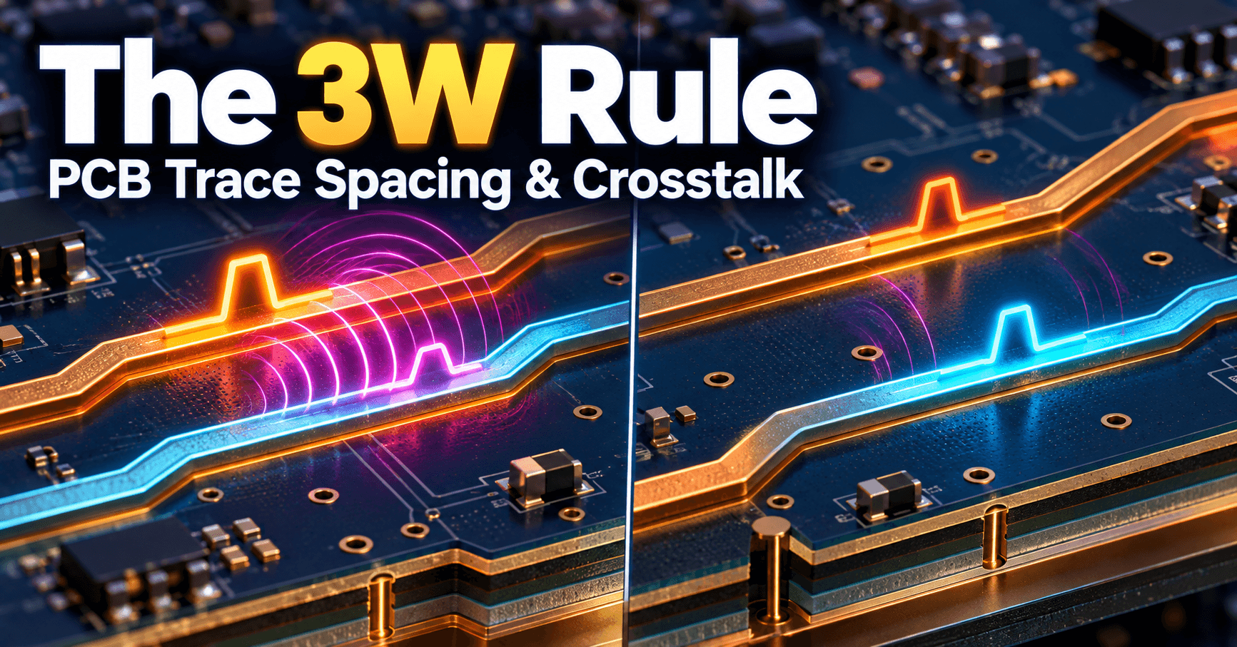
Crosstalk is the price you pay for routing two traces near each other. Every signal trace radiates a fringing electric field and a magnetic field around it, and any neighboring trace sitting inside that field picks up a fraction of the aggressor's energy as induced noise. The 3W rule is a layout heuristic that says: if you space traces so that the distance between their centerlines is at least three times the trace width (S = 3W), the coupled noise drops to a level that's usually negligible for digital logic. It originated in empirical PCB design practice (documented in IPC-2141 and widely repeated in signal integrity texts) rather than from a closed-form derivation — it's a field-engineering rule of thumb, not a law of physics.
The cost of ignoring trace spacing
Ignoring spacing doesn't fail quietly. A board that passes bench testing at room temperature can fail in the field when a clock edge sharpens due to a driver IC lot change, when supply voltage droops and noise margins shrink, or when a neighboring aggressor trace carries a different data pattern that happens to align with a victim's sampling window. The failure shows up as intermittent bit errors, EMI test failures, or a DDR training routine that works on 9 boards out of 10. Debugging it after the fact means rework: cutting traces, bodging in series resistors, or respinning the board — all far more expensive than adding 2 mils of spacing during layout.
When crosstalk becomes a signal integrity crisis
Crosstalk is a nuisance until it eats directly into your timing or voltage margin. On a single-ended bus with 400 mV of noise margin, even 50–80 mV of induced crosstalk from an aggressor clock can be the difference between a clean eye and a marginal one. The crisis point is reached when coupled noise, combined with reflection noise from impedance mismatches and ISI from the channel, exceeds the receiver's margin budget. At that point it's not a cosmetic issue — it's a bit-error-rate problem.
Real-world failure modes in DDR and SerDes systems
In DDR systems, the classic failure is a clock or strobe (CLK/DQS) routed too close to an address or command line, injecting enough edge noise to cause intermittent read/write training failures that look like a timing bug. In SerDes systems, tightly packed differential pairs routed near single-ended control signals can couple enough common-mode noise to degrade jitter past the receiver's tolerance, especially at multi-Gbps rates where unit intervals are tens of picoseconds wide.
Understanding the 3W Formula
What W represents: trace width and its role
W is the trace's copper width, which is set by your controlled-impedance stackup calculation (typically 4–6 mils for 50 Ω single-ended traces on common stackups, but always verify against your fab's impedance calculator). Because trace width also defines field spread — the narrower the trace, the more tightly its field is bound near the surface — using W as the spacing reference automatically scales separation with the geometry that's actually generating the field.
How separation distance S = 3W was derived
S = 3W comes from empirical field measurements showing that roughly 70% of a microstrip trace's electric field flux falls within one trace-width's distance from its edge, and nearly all practically coupled energy falls within a 3W radius. The rule bundles this observation into a single multiplier so designers don't need a field solver for routine digital routing. It's conservative by design — a working approximation good enough to catch the overwhelming majority of coupling problems without requiring EM simulation on every net.
Why 3× provides safety margin vs. 2× or 1× spacing
Coupling doesn't scale linearly with spacing — it falls off roughly with distance due to field decay, so even small increases in spacing produce disproportionate reductions in coupled noise close to the trace, with diminishing returns farther out. Going from 1W to 2W spacing captures a large share of possible noise reduction; going from 2W to 3W adds a meaningful additional margin for a comparatively small area cost. Beyond 3W, each additional W buys progressively less noise reduction, which is why 3W is treated as the practical "good enough" point rather than 5W or 10W: it's near the knee of the coupling-vs-distance curve.
Coupling coefficient and field decay in practice
Think of the coupling coefficient as an attenuation factor applied to the aggressor's switching energy. At 1W spacing, induced crosstalk on an adjacent victim can commonly run several percent of the aggressor's swing — enough to matter on tight-margin buses. At 3W, that figure typically drops to a fraction of a percent to low single digits, depending on dielectric height and trace geometry. These are order-of-magnitude guides, not guaranteed numbers — confirm actual coupling with a field solver or your stackup vendor's impedance/crosstalk tool for anything timing-critical.
Crosstalk Mechanisms: Capacitive vs. Inductive
Near-end and far-end crosstalk defined
Near-end crosstalk (NEXT) appears at the victim trace's end closest to the aggressor's driver, caused mainly by capacitive coupling; it builds up as a pulse that travels back toward the aggressor's source. Far-end crosstalk (FEXT) appears at the victim's far end, driven by the difference between capacitive and inductive coupling, and its polarity and magnitude depend on whether the dominant coupling is capacitive or inductive dominant — on a symmetric stripline structure with matched coupling, FEXT can even cancel.
How trace separation reduces both coupling paths
Increasing S reduces both the mutual capacitance Cm and mutual inductance Lm between traces, since both terms fall off with the inverse of separation distance raised to some power dependent on geometry. Wider spacing weakens both the electric (capacitive) and magnetic (inductive) coupling paths simultaneously, which is why 3W works as a single rule rather than needing separate capacitive and inductive spacing rules.
Trade-offs: spacing vs. board density
Every mil of spacing is a mil you don't have for routing channels, via fanout, or layer count reduction. On a dense DDR4 memory interface with 50+ single-ended signals per byte lane, strictly applying 3W everywhere can force an extra routing layer, directly increasing board cost. This is where engineering judgment — knowing which nets are noise-sensitive and which aren't — pays for itself.
When 3W is insufficient (high-speed > 5 Gbps)
Above roughly 5 Gbps, the unit interval shrinks enough that even sub-percent crosstalk can erode jitter budgets, and discontinuities that were invisible at lower speeds (vias, connector transitions, stub lengths) start dominating signal integrity. At these rates, 3W should be treated as a starting point, not a sign-off criterion — PCIe Gen4/5, 10G+ SerDes, and similar interfaces require full-channel simulation, including the effects described by Two-Port Network Parameters: Z, Y, H, ABCD to model coupled-line behavior properly, rather than relying on a width-ratio heuristic.
Applying 3W in Real Layouts
DDR4 address bus and clock routing under 3W
On a DDR4 byte lane, apply 3W rigorously to CLK/CLK# and DQS/DQS# relative to address, command, and data lines — these are the nets most sensitive to injected noise because they define sampling edges. Address and command lines routed next to each other at 3W are generally safe for typical DDR4 speeds, but always check your memory controller vendor's layout guideline document for the actual required spacing, since some specify tighter or looser rules than the generic 3W heuristic.
Differential pair spacing and the 3W exception
Differential pairs are the one place 3W is deliberately broken: the two traces of a pair are routed intentionally close together (often 1W to 2W apart) to maintain tight coupling and common-mode rejection. The 3W rule then applies between the pair as a unit and other nets — treat the pair's outer edges as the reference and keep 3W (measured from the pair, not from each individual trace) to adjacent aggressors.
Layer stackup impact on required separation
Dielectric height between the trace and its reference plane changes how tightly the field is bound to the trace. A trace on a thin dielectric (close to its plane) has a more tightly confined field and needs less spacing for the same crosstalk performance; a trace on a thick dielectric (far from its plane) spreads its field wider and may need more than 3W to hit the same target. If your stackup uses unusually thick core or prepreg layers, don't assume generic 3W values from a different stackup transfer directly — rerun the field solver for your actual dielectric height.
Via stitching and guard traces as alternatives
Where density prevents full 3W spacing, a grounded guard trace between aggressor and victim, stitched to the reference plane with vias every fraction of a wavelength, intercepts fringing fields and provides a return path close to the signal, cutting coupling without consuming as much lateral space as doubling the gap would.
Design Trade-offs and Exceptions
When to use tighter spacing (controlled impedance, matched lengths)
Length-matched serpentine groups and controlled-impedance differential pairs routinely violate 3W by design, because the coupling is either intentional (differential pairs) or because the signals are low-risk (matched clock trees on low-speed buses where skew matters more than isolation). The decision to go tighter should be based on an actual noise budget calculation, not convenience.
Low-speed logic signals that ignore 3W
GPIOs, reset lines, I2C, low-speed SPI, and similar sub-10 MHz signals rarely need 3W spacing at all — their edge rates are slow enough that induced crosstalk energy is negligible relative to their noise margins. Applying 3W there is over-design that burns routing density for no SI benefit.
Power and ground plane effects on coupling
A solid, uninterrupted reference plane under a signal layer reduces crosstalk by giving the return current a direct, low-impedance path directly beneath the trace, concentrating the field between trace and plane rather than letting it spread sideways to a neighbor. Split planes or plane gaps under high-speed traces defeat this benefit and can make a 3W-spaced layout behave like a much tighter one.
Cost vs. signal integrity in volume production
In high-volume consumer products, every extra square millimeter and every added layer has a recurring cost multiplied across millions of units. The 3W rule gives a defensible, low-effort default; deviating from it to save board area should be backed by simulation or measurement data, not just schedule pressure — rework after production start is far costlier than a layer added at design time.
Verification and Measurement
Identifying crosstalk in simulation before layout
Pre-layout, 2D field solvers (often bundled into PCB tools or stackup calculators) estimate coupling coefficients for a proposed trace geometry before a single trace is drawn, letting you catch problems in the stackup decision stage rather than after routing is complete.
Design rule checks (DRC) for trace spacing enforcement
Most PCB layout tools support spacing-class DRC rules that can enforce a minimum S relative to W, or a flat minimum spacing per net class (clocks, differential pairs, DDR address/data). Define these classes early and let the DRC catch violations continuously rather than relying on a manual spacing audit at the end — the same discipline that applies to enforcing Annular Ring: IPC-6012 Minimum Ring Requirement constraints on vias.
Lab measurement: TDR and network analyzer validation
Post-fabrication, a time-domain reflectometer (TDR) with coupled-line probing or a vector network analyzer measuring near-end and far-end coupling (S21/S31-style parameters between aggressor and victim ports) validates whether actual coupling matches simulation. Differences usually point to stackup variation (actual dielectric thickness or Dk differing from nominal) rather than a layout error.
Post-layout refinement and rework constraints
Once a board is routed and fabricated, your rework options are limited: adding a guard trace means a new spin; moving traces apart may not be possible without re-routing an entire section. This is why spacing violations should be caught in DRC or simulation, not discovered during bring-up.
Beyond 3W: Advanced Mitigation Techniques
Guard traces and Faraday shielding principles
A grounded guard trace stitched to the plane with vias at intervals well below the signal's effective wavelength acts as a partial Faraday shield, intercepting fringing field lines before they reach the victim. It's most effective against capacitive coupling and less effective against inductive coupling at high frequency unless via stitching density is high.
Layer assignment strategies to break coupling
Routing aggressor and victim on different layers, separated by a reference plane, breaks direct coupling far more effectively than lateral spacing on the same layer — the plane acts as a shield. This is often cheaper in board area than widening spacing, at the cost of an extra via transition per crossing.
Serpentine routing and phase alignment
When length-matching forces serpentine routing near other signals, keep the serpentine's self-coupling (adjacent legs of the same trace) in mind as well — tight serpentine turns can couple to themselves, and the same 3W-style spacing logic (and the coupling math behind Voltage Divider and Current Divider Rules when estimating injected noise as a fraction of swing) applies within a single net's folded geometry, not just between separate nets.
When to combine 3W with termination and equalization
At the data rates where 3W alone is insufficient, pair adequate spacing with series or parallel termination to control reflection-driven noise, and consider receiver equalization to recover margin lost to residual coupling. 3W reduces the crosstalk term in the margin budget; termination and equalization address the reflection and ISI terms — a complete high-speed design needs all three addressed together, not 3W treated as a standalone fix.
Learning
Sign in to track your progress.
Evidence
Public projects engineers linked to 3W Rule: Trace Separation = 3× Trace Width to Reduce Crosstalk.
No engineer has linked a project to this topic yet. Built something that proves it? Add the project and tag it with pcb-and-3w-rule-trace-separation-3-trace-width-to-reduce-c — it then shows here and on your public profile.