
Switching Transients: VDS/VGS Overshoot, Ringing
Understand VDS/VGS overshoot and ringing causes, measurement pitfalls, and layout/snubber fixes for reliable power switch designs.
Contents & prerequisites
Why Overshoot and Ringing Occur
Energy storage in parasitic inductances during switching
Every trace, bond wire, and package lead in a power stage carries inductance, typically 1–20 nH per cm of PCB trace and a few nH per device package. During a hard commutation, the switch current changes from zero to full load current (or back) in tens of nanoseconds. That di/dt forces energy into the parasitic loop inductance, E = ½ L I². When the switch then tries to interrupt that current abruptly, the inductance resists the change and generates a voltage spike V = L(di/dt) superimposed on the DC bus. This is the single most common root cause of VDS overshoot in MOSFETs and IGBTs.
The role of device output capacitance (Coss) in transient behavior
The switch itself is not a pure switch—it has a nonlinear output capacitance, Coss, that varies strongly with VDS (often 5–10x higher at low voltage than at rated voltage). Coss must charge or discharge during each transition, and it forms an LC tank with the loop inductance. The stored energy in the parasitic inductance doesn't just disappear when current stops flowing; it transfers into Coss, producing the voltage overshoot, and then rings back and forth between L and C until damped by resistive losses.
Voltage spike formation: stored energy redistribution
Think of the turn-off transition as an energy-handoff problem: inductive energy ½LI² converts into capacitive energy ½CV², so the peak excess voltage above the bus is approximately ΔV ≈ I·√(L/C). This single relationship explains why high-current, fast designs with long power loops see the worst spikes—both I and L sit in the numerator.
Time-domain mechanisms in hard-switching topologies
In a hard-switched buck, half-bridge, or motor-drive leg, the diode or synchronous MOSFET reverse recovery adds a second spike source: the recovery current must also be interrupted, dumping additional energy into the same loop inductance. The result is a compound event—first the turn-off spike, then a secondary ring triggered by recovery—visible on a scope as two overlapping decaying sinusoids before settling to steady state.
VDS Overshoot: Drain-Source Voltage Transients
Peak voltage exceeding DC bus: how much and why
A clean 400 V bus design can easily show 480–550 V instantaneous VDS peaks with a poorly laid-out loop and fast switching edges. The overshoot magnitude depends on loop inductance, switched current, and Coss at the relevant voltage—there is no fixed percentage rule; it must be measured or simulated for each design.
Ringing waveforms after initial overshoot
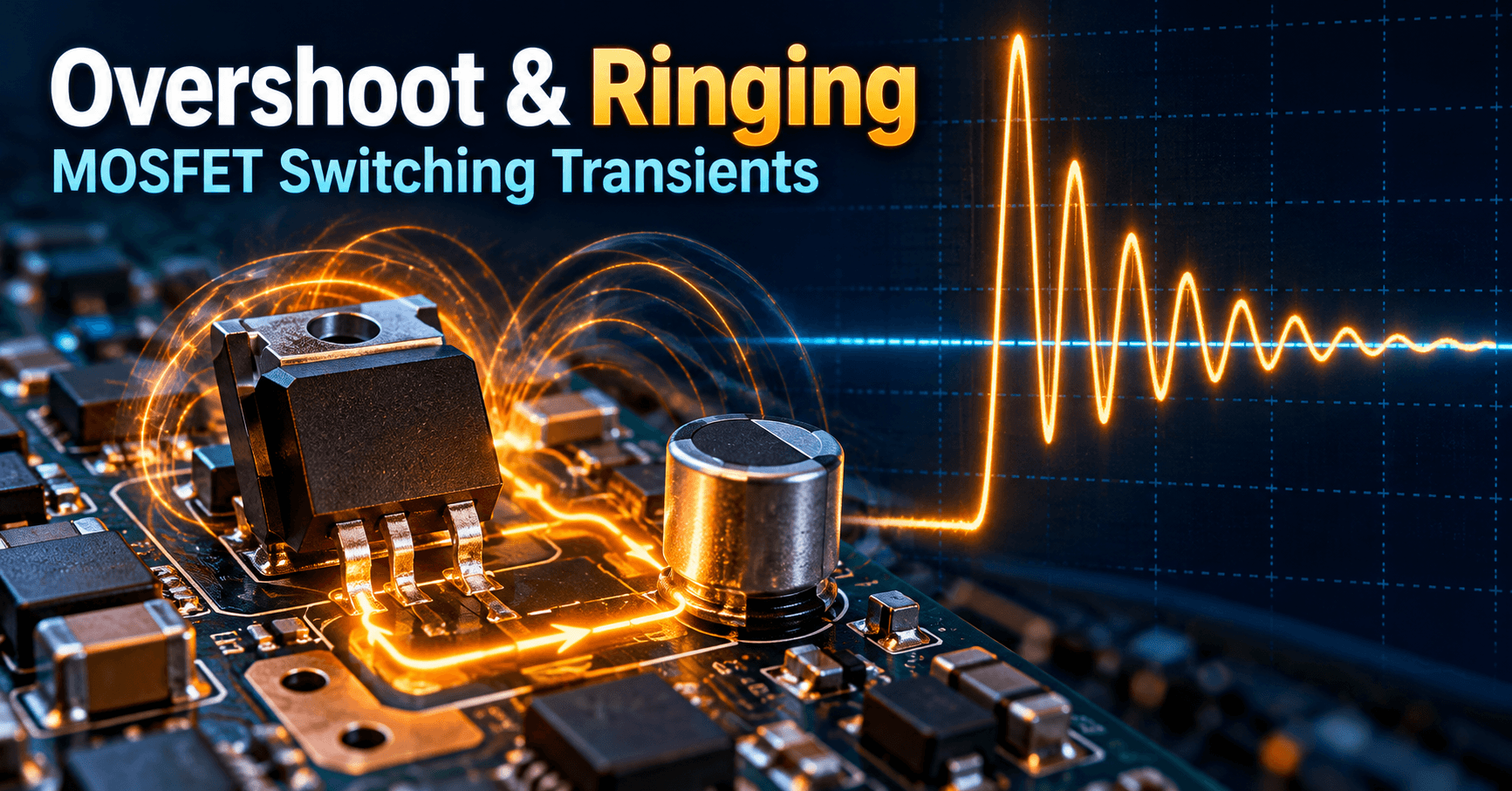
After the initial peak, the LC tank rings at its natural frequency, decaying exponentially as loop resistance and switch output resistance dissipate the stored energy. Ring frequencies commonly fall between 20 MHz and 150 MHz for discrete power stages, well above the switching frequency itself, which is why they're invisible on low-bandwidth measurement setups.
Relationship between switching speed (dI/dt, dV/dt) and peak stress
Faster edges reduce switching loss but increase both di/dt (driving inductive spikes) and dV/dt (driving capacitive displacement currents and EMI). This is the central trade-off in gate drive design: slowing the edge lowers the overshoot term L(di/dt) but raises conduction overlap loss. Quantitatively, halving the current transition time roughly doubles the inductive spike contribution for a fixed L.
Impact on device ratings and safe operating area (SOA)
Repeated excursions near or above the VDS absolute maximum rating degrade the device even if it doesn't fail immediately—avalanche events stress the junction edge termination and can shift threshold voltage over time. SOA curves in datasheets assume controlled, single-pulse conditions; transient ringing events are rarely characterized there, so designers must budget margin separately using the device's reverse-bias breakdown behavior described in Reverse Bias: Leakage Current, Breakdown Mechanisms.
Measurement challenges and probe considerations
A standard 10:1 passive probe with a 6-inch ground lead has enough loop inductance to self-resonate below 100 MHz—exactly where real ringing occurs—making it impossible to tell probe artifact from device behavior without care (see the measurement section below).
VGS Overshoot: Gate-Source Voltage Transients
Gate voltage excursions beyond target bias
VGS is not immune to transients. Even with a stable gate driver output, the actual gate-source voltage at the die can overshoot the intended level by several volts during fast drain transitions, especially in high-side switches in half-bridge legs.
Coupling mechanisms: capacitive coupling from drain switching
The Miller capacitance (Cgd) couples drain dV/dt directly into the gate node. When the opposing switch turns on and forces a fast dV/dt across the off-state device, displacement current flows through Cgd into the gate loop. If the gate drive impedance is too high, this current develops enough voltage to partially turn the device back on (Miller turn-on) or exceed the VGS rating.
Risk of unwanted gate-source current and breakdown
Gate oxide breakdown voltages are typically in the 20–25 V range for modern power MOSFETs, with no significant avalanche capability—unlike the drain-source junction. A brief VGS spike exceeding this rating can cause instant, permanent gate rupture, which is why VGS transients deserve equal attention to VDS transients despite the lower voltage magnitude.
Gate drive design influence on VGS stability
Gate drive loop inductance, driver output impedance, and a solid low-impedance return path from gate drive return to source (Kelvin source) all affect how much the gate rings. A driver with low pull-down impedance and a dedicated Kelvin connection substantially reduces Miller-induced overshoot compared to a shared power-source return.
Root Causes: Inductance and Capacitance Resonance
PCB loop inductance as the primary culprit
In nearly every production failure investigation involving overshoot, the dominant contributor traces back to PCB power loop area—not the device itself. A detailed treatment of loop inductance estimation and Coss interaction is covered in Device Parasitics: PCB Loop Inductance, Coss Resonance.
Device output capacitance (Coss) resonating with circuit inductance
Because Coss is voltage-dependent, the resonant frequency actually shifts during the ringing event—higher near the voltage peak (low Coss) and lower near the troughs (high Coss)—so real ring waveforms are not pure sinusoids but slightly chirped decaying oscillations.
LC resonant frequency prediction and measurement
A first-order estimate: f = 1/(2π√(L·Ceff)). For example, with 15 nH of loop inductance and an effective Coss of 150 pF, f ≈ 1/(2π√(15e-9 × 150e-12)) ≈ 106 MHz. Measuring the actual ring period on a scope and back-solving for L (with Coss taken from the datasheet curve) is a standard way to validate a layout's parasitic inductance.
Damping ratio and Q-factor effects on ringing severity
The loop's series resistance (trace resistance, device Rds(on), ESR of decoupling caps) sets the damping ratio ζ = R/2·√(C/L). Low-ESR layouts with minimal resistance ring longer and harder; counterintuitively, adding a small resistive element (an RC snubber) deliberately lowers Q and shortens the ringing duration at a modest efficiency cost.
Practical Mitigation Strategies
PCB layout: minimizing current loop area
The highest-leverage fix is geometric: route the decoupling capacitor, switch, and return path as a tight, overlapping loop, ideally using adjacent layers with the forward and return current directly above/below each other. Cutting loop area in half roughly halves the loop inductance.
Snubber networks and clamp diodes
An RC snubber across the switch or an RCD clamp across a transformer winding absorbs the inductive energy resistively instead of letting it ring. Snubber component sizing follows directly from the energy and resonance equations above—start from the measured ring frequency and work backward to the effective L and C, a process analogous to the impedance-matching math used in Two-Port Network Parameters: Z, Y, H, ABCD, since a snubber is effectively a network inserted to reshape the loop's impedance response.
Gate resistor tuning for controlled dV/dt
Increasing the gate resistor slows both turn-on and turn-off edges, trading switching loss for reduced overshoot. Many designs use asymmetric gate resistors (separate turn-on and turn-off paths with a diode) to control dV/dt and di/dt independently.
Soft-switching topologies as an alternative
Zero-voltage-switching (ZVS) or zero-current-switching (ZCS) topologies avoid the hard interruption of current/voltage altogether, eliminating the energy-dump mechanism rather than damping it after the fact—worth considering when transient mitigation in a hard-switched design becomes a losing trade-off.
Reliability and Design Implications
Overvoltage stress shortening device lifetime
Even sub-breakdown overshoot events cause cumulative stress through hot-carrier injection and localized heating at the junction periphery, shortening time-to-failure in ways that single-pulse datasheet ratings do not capture.
EMI generation from transient voltage edges
Ringing at tens of MHz couples efficiently into nearby traces and radiates, often the direct cause of conducted and radiated EMI test failures; damping the ring reduces both device stress and emissions simultaneously.
Gate oxide stress from VGS overshoot
Unlike drain-source avalanche, gate oxide damage is cumulative and non-recoverable—repeated near-threshold excursions can shift Vgs(th) gradually before outright failure, making VGS margin a reliability issue even without a single catastrophic event.
Trade-offs: reducing transients vs. switching losses
Every mitigation technique—slower edges, snubbers, soft switching—trades some efficiency or cost for reduced stress. The right balance point is set by the application's thermal budget and reliability target, not by a single rule of thumb.
Simulation and Measurement Techniques
SPICE modeling of parasitic inductance and capacitance
Extract loop inductance from PCB field solvers or from the physical geometry (trace width, spacing, layer stackup), and add it along with the manufacturer's nonlinear Coss model (often provided as a SPICE subcircuit) to predict ringing before board spin. A quick hand-check, as shown in the resonance section, catches gross errors before running full simulation.
High-bandwidth oscilloscope probing for VDS and VGS
Use probes with bandwidth at least 3–5x the expected ring frequency, and minimize probe ground lead length—often by using a compensated low-inductance tip-and-barrel ground spring instead of a long ground clip.
Distinguishing real overshoot from probe ringing artifacts
A quick diagnostic: touch the probe tip directly to the ground plane near the measurement point with the shortest possible ground path and observe residual noise; if the "ringing" amplitude or frequency changes significantly with ground lead length, it's probe-induced, not device-induced.
Time-domain verification of mitigation effectiveness
After adding a snubber or adjusting gate resistance, re-measure peak VDS/VGS and ring duration under the same load and bus voltage conditions used in the original characterization—changing the measurement conditions alongside the fix (a common mistake analogous to misapplying Voltage Divider and Current Divider Rules without accounting for loading effects) will produce misleading before/after comparisons.
Learning
Sign in to track your progress.
Evidence
Public projects engineers linked to Switching Transients: VDS/VGS Overshoot, Ringing.
No engineer has linked a project to this topic yet. Built something that proves it? Add the project and tag it with power-electronics-switching-transients-vdsvgs-overshoot-ringing — it then shows here and on your public profile.