
Gate Drive: Bootstrap, Optocoupler, Isolated IC
Gate drive isolation compared: bootstrap, optocoupler, and isolated IC architectures, with design rules for frequency, dV/dt, and reliability.
Contents & prerequisites
Why Gate Drive Isolation Matters
Floating gate nodes in half-bridge and full-bridge topologies
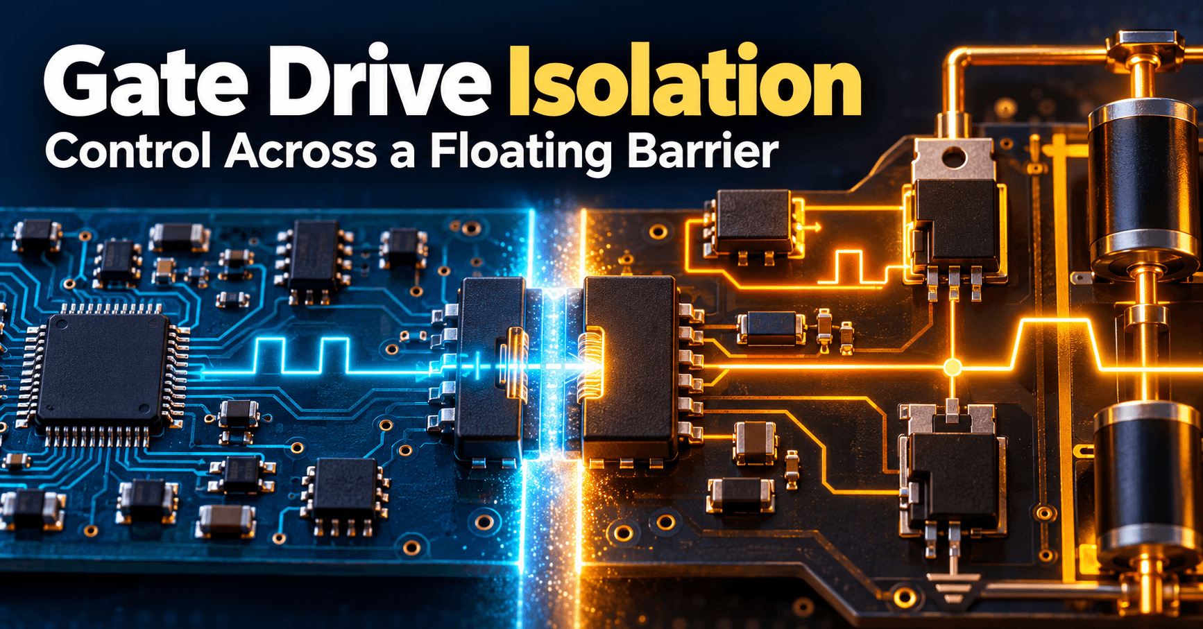
In a half-bridge leg, the high-side MOSFET or IGBT source (or emitter) node swings between the negative and positive rail every switching cycle. The gate drive referenced to that node has no fixed ground — it rides on the switch node, which can move hundreds of volts in tens of nanoseconds. Any control signal generated in a fixed-ground PWM controller must somehow cross into this floating domain without dragging the switch node back to controller ground through a low-impedance path. That crossing is the isolation problem, and every gate drive architecture—bootstrap, optocoupler, or isolated IC—is really just a different answer to "how do I move a logic edge across a moving reference without shorting it."
Common-mode voltage stress and noise immunity
The isolation barrier sees two stresses simultaneously: the absolute common-mode voltage (how far the floating node sits from ground, often the full bus voltage) and the common-mode transient, dV/dt, during each switching edge. A barrier rated for working voltage may still fail under high dV/dt if its parasitic coupling capacitance injects enough displacement current to false-trigger logic on the other side. This is why driver datasheets specify a CMTI (common-mode transient immunity) figure in kV/µs, not just an isolation voltage rating — look up the CMTI number in the specific driver's datasheet before committing to a part for a fast SiC or GaN design.
Safety and reliability trade-offs in isolated vs. non-isolated designs
Non-isolated (bootstrap) drive is not "unsafe" in the UL/IEC sense if the bootstrap diode and capacitor are rated for the full bus voltage, but it offers no galvanic barrier between control logic and power stage — a gate-source short or avalanche event can propagate back toward the controller. True isolation (optocoupler, transformer, or capacitive) breaks that path and is often mandated by safety standards (e.g., basic or reinforced isolation per IEC 60747-5-5 or IEC 60664-1) in mains-connected or human-accessible equipment. The decision is therefore not purely technical; it's also a compliance question that should be settled before topology lock-in.
Bootstrap Gate Drive Fundamentals
Principle: capacitive coupling for floating high-side gate
A bootstrap circuit uses a small capacitor referenced between the high-side driver's floating supply pin and the switch node, charged through a diode from a low-side fixed rail (typically VCC) whenever the switch node is pulled low. The capacitor becomes a local, floating battery that supplies gate charge for the high-side turn-on, even though its "ground" is moving.
Charge and discharge cycle during switching transitions
When the low-side device conducts, the switch node sits near ground and the bootstrap diode conducts, charging the capacitor to roughly VCC minus the diode drop (recall the exponential I-V relationship near turn-on described in Forward Bias: Exponential Current, Knee Voltage, which sets how much headroom you lose to the diode's knee voltage at your actual charging current). When the high-side device turns on, the switch node rises with the bus, the diode blocks, and the capacitor alone must supply the gate charge Qg for that turn-on plus any quiescent bias current drawn by the high-side driver during the on-time.
Limitations: minimum on-time, charge loss, and refresh requirements
Every switching cycle drains the bootstrap capacitor by Qg plus leakage; it can only be replenished during low-side conduction. This creates two related constraints: a maximum duty cycle (the high side can't stay on indefinitely, or the cap droops below the driver's undervoltage lockout) and a minimum low-side on-time (the cap needs enough low-side conduction time each cycle to recharge). Extreme duty cycles near 0% or 100% are therefore problematic. A simple sizing check: for gate charge Qg, switching frequency f, and allowable droop ΔV, the minimum capacitance is
C_boot >= Qg / ΔV
with ΔV typically kept to 5–10% of the drive voltage. Add margin for diode and driver quiescent current, and verify against the low-side minimum on-time at your actual duty cycle range, not just at 50%.
Best-case applications: PWM converters with bounded duty cycle
Bootstrap drive is the right default for boost converters, buck converters, and other single-switch or half-bridge topologies where duty cycle stays within a known band and the circuit isn't expected to park at extreme duty ratios for long intervals. It's cheap, requires no isolated supply, and is well supported by integrated half-bridge driver ICs.
Optocoupler-Based Isolation
LED–photodiode isolation barrier and propagation delay
An optocoupler transmits the gate command as light across a dielectric gap: an LED on the primary (controller) side drives a photodiode or phototransistor on the secondary (floating) side. This gives true galvanic isolation, but the LED-to-photodiode conversion and the following amplifier stage add propagation delay, typically on the order of 100 ns to several hundred ns depending on the part, with delay varying with temperature and LED drive current.
Advantages: low cost, simple integration, adequate for low-speed applications
For line-frequency or low-kHz switching—motor soft-starters, legacy IGBT drives, relay-adjacent logic—optocouplers remain attractive: inexpensive, available in through-hole and SMD, and well understood by several generations of power engineers.
Disadvantages: temperature drift, CTR variation, and speed limitations
Current transfer ratio (CTR) — the ratio of output photocurrent to input LED current — degrades with LED aging and temperature, often dropping 20–50% over the component's operating lifetime depending on LED drive current and junction temperature. A design that worked at CTR = 100% at room temperature may fail to fully turn on the output transistor after years of operation at elevated temperature. This aging margin must be designed in up front, not patched in later, and it's a primary reason optocouplers are losing ground in new high-reliability designs to isolated ICs.
Practical design: pull-up resistor sizing and output buffer stage
The output-side pull-up resistor sets both the output voltage swing and the switching speed; too large a value slows the rising edge (dominated by stray capacitance and pull-up RC), too small wastes power and increases minimum CTR requirements. Most practical designs buffer the optocoupler's open-collector output with a small push-pull stage or Schmitt-trigger gate before it drives the power MOSFET/IGBT gate, since the optocoupler alone usually cannot source enough current to charge gate capacitance quickly. The same loading math that governs resistor selection in general analog stages — see Voltage Divider and Current Divider Rules — applies directly here when sizing the pull-up against the downstream buffer's input impedance.
Isolated Gate Driver ICs
Monolithic isolation: capacitive and magnetic coupling technologies
Modern isolated gate driver ICs replace the LED-photodiode pair with on-chip capacitive (SiO2 or polyimide dielectric) or magnetic (integrated transformer) coupling, encoding the logic signal as a high-frequency pulse pair rather than a DC light level. This sidesteps CTR aging entirely and allows much higher data rates across the barrier.
Integration benefits: integrated charge pump, programmable dead-time, diagnostics
Beyond isolation, these parts commonly integrate an internal charge pump (removing the bootstrap diode/capacitor entirely for some topologies), programmable dead-time generation, desaturation (desat) fault detection for IGBTs, undervoltage lockout on both primary and secondary sides, and fault feedback across the barrier — functions that would otherwise require discrete circuitry analyzable with Two-Port Network Parameters: Z, Y, H, ABCD if built from separate gain and feedback stages.
Speed and noise performance: sub-100 ns propagation delay and high dV/dt immunity
Capacitive and magnetic isolators typically achieve propagation delays under 100 ns with part-to-part skew measured in single-digit nanoseconds, and CMTI ratings often exceeding 100 kV/µs — figures you should confirm against the specific part's datasheet, since they vary significantly by isolation technology and voltage rating.
Multi-channel scalability for three-phase and modular applications
Multi-channel isolated driver ICs (three or six channels in one package) simplify three-phase inverter and modular multilevel designs by matching propagation delay across channels, which matters more than any single channel's absolute delay when you're trying to keep phase-leg timing symmetric.
Comparison: Cost, Speed, and Reliability
Bootstrap: lowest cost, limited frequency and duty-cycle range
Lowest component count and cost, no isolated bias supply needed, but bounded by duty-cycle and minimum on-time constraints, and it offers no galvanic isolation — a fault on the floating side can reflect into the controller rail.
Optocoupler: mid-range cost and performance, aging and temperature sensitivity
True isolation at moderate cost, but propagation delay, CTR aging, and temperature sensitivity limit it to lower switching frequencies and less demanding timing budgets.
Isolated IC: highest cost, best performance and integration, long lifetime
Highest unit cost but lowest total system cost in many designs once you account for eliminated discrete components, built-in diagnostics, and the multi-year stability of capacitive/magnetic coupling versus LED degradation.
Selection Criteria and Design Tradeoffs
Switching frequency, modulation scheme, and continuous operation requirements
High switching frequency (hundreds of kHz and above, common with SiC/GaN) generally rules out optocouplers on propagation-delay and timing-jitter grounds, and may stress bootstrap duty-cycle limits if the modulation scheme calls for sustained high duty ratio.
Common-mode dV/dt environment and EMI robustness
Fast-edge devices push dV/dt well above what legacy optocouplers were characterized for; this is the central reason isolated ICs with explicit CMTI specs have displaced optocouplers in new SiC/GaN designs, independent of switching frequency alone.
PCB layout, power supply isolation, and feedback loop implementation
Isolation barriers must be matched by physical creepage/clearance on the PCB and by an isolated bias supply (transformer-based DC-DC or similar) for optocoupler and IC solutions; skimping on layout isolation defeats the component-level isolation rating.
Thermal derating and long-term reliability expectations
Optocoupler CTR derating over temperature and lifetime should be built into the worst-case gate drive current budget; isolated ICs still require junction temperature derating per their datasheet but without the CTR aging variable.
Practical Integration Considerations
Gate resistor and Miller effect interaction with drive architecture
Gate resistor selection interacts with Miller plateau behavior regardless of isolation technique: too high a resistance slows the Miller transition and increases switching loss and dV/dt-induced noise coupling back into the isolation barrier; too low increases ringing and EMI.
Decoupling and power distribution for low-impedance gate current
Place bypass capacitance directly at the driver's floating supply pins; gate charge current pulses are large and fast, and any inductance in the decoupling path shows up as supply droop at the gate during turn-on.
Fault detection and shutdown logic in isolated topologies
Isolated driver ICs with desat or current-sense feedback need a defined fault-propagation path back across the barrier with bounded latency; design the shutdown logic (and its own small feedback loop, conceptually similar to compensation networks built around op-amp stages like the one in Two-Stage Op-Amp: Differential Input + Common-Source Output) so that a fault doesn't itself inject a false reset during the recovery transient.
Example scenarios: boost converter (bootstrap), three-phase inverter (isolated IC)
A single-switch boost converter at 100 kHz with duty cycle bounded between 20–80% is a textbook bootstrap application: compute Qg from the MOSFET datasheet, size C_boot per the droop formula above, and confirm the diode's forward drop doesn't starve the cap at minimum on-time. A three-phase SiC inverter switching at 50–200 kHz with fast edges, by contrast, calls for isolated gate driver ICs on all six switches, chosen for CMTI margin above the expected dV/dt and matched propagation delay across channels to preserve phase symmetry.
Learning
Sign in to track your progress.
Evidence
Public projects engineers linked to Gate Drive: Bootstrap, Optocoupler, Isolated IC.
No engineer has linked a project to this topic yet. Built something that proves it? Add the project and tag it with power-electronics-gate-drive-bootstrap-optocoupler-isolated-ic — it then shows here and on your public profile.