
Bare Board Incoming Inspection per IPC-A-600
Bare board incoming inspection per IPC-A-600: learn the defect checks, acceptability classes, and test methods that prevent assembly rework.
Contents & prerequisites
What Is Bare Board Incoming Inspection?
Bare board incoming inspection is the formal check of unpopulated printed circuit boards (PCBs) against a documented standard before they enter the assembly line. It happens at receiving, after the boards arrive from the fabricator and before kitting, solder paste printing, or pick-and-place programming begins. The goal is simple: confirm that what you received is what you specified, and that it will survive reflow and functional test.
Purpose and timing in the assembly workflow
Inspection should occur immediately on receipt, ahead of any work order release. Once a board has been through solder paste printing and placement, every defect found costs far more to fix — you've now got scrap components, operator time, and schedule slip stacked on top of the bare board cost. A typical placed and reflowed board can represent 10-50x the material cost of the bare board alone, so incoming inspection is the cheapest point at which to catch a defect.
Why inspection before component placement matters
A cracked laminate, an underetched trace, or a via with insufficient copper wrap can pass a quick visual glance but fail catastrophically during reflow thermal cycling or in the field under vibration. Once components are soldered down, rework to replace a board means desoldering good parts, risking thermal damage to pads, and potentially scrapping expensive BGAs or fine-pitch parts that can't be reused. Incoming inspection is the last point where a bad board can be rejected at near-zero sunk cost.
Role of IPC-A-600 standard
IPC-A-600, "Acceptability of Printed Boards," is the industry reference for what counts as a defect on a bare (unpopulated) PCB. It defines target, acceptable, and nonconforming conditions for dozens of board features — plating, drilling, solder mask, laminate — using photographs and line drawings so inspectors across companies apply the same criteria. It does not test electrical performance (that's IPC-9252 territory) or assembly workmanship (IPC-A-610); it is strictly about the fabricated board itself.
IPC-A-600 Acceptability Standards Overview
Three acceptability classes: 1, 2, and 3
IPC-A-600 criteria are tied to the IPC-6012 (rigid board performance) class system:
- Class 1 — General Electronic Products. Cost and schedule dominate; cosmetic and minor dimensional variances are tolerated as long as function isn't compromised.
- Class 2 — Dedicated Service Electronic Products. Reliability and extended service life matter; this is the default for most industrial and commercial equipment.
- Class 3 — High Reliability Electronic Products. Continued performance or performance-on-demand is critical — medical implants, avionics, military systems. Tightest tolerances, zero tolerance for many defects acceptable in Class 2.
How class selection drives inspection rigor
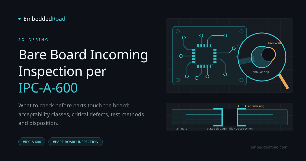
The class isn't chosen at inspection time — it should already be called out on the fabrication drawing or purchase spec per IPC-6012. The inspector's job is to apply the matching IPC-A-600 acceptance tables for that class. The same physical defect (say, a 90° annular ring breakout on a plated through-hole) may be acceptable on a Class 1 or Class 2 board and a reject on a Class 3 board, which requires an intact external annular ring of at least 0.050 mm (0.002"). If your incoming inspection procedure doesn't reference a class, that's a gap to close before you inspect a single board — ambiguity here is the single most common cause of inspector-to-inspector disagreement.
Defect classification levels
Within each class, IPC-A-600 categorizes conditions as:
- Target — the ideal, fully-conforming condition.
- Acceptable — meets minimum requirements, may show minor cosmetic variance.
- Nonconforming — fails requirements and should be rejected, reworked (if possible), or sent back with a nonconformance report.
Critical Bare Board Defects to Inspect
Conductor spacing and trace width violations
Check minimum conductor spacing and width against the fab drawing and the applicable IPC-6012 class table. Underetched traces (too wide, too close) risk shorts or reduced impedance margin; overetched traces (too narrow) risk current density issues and fusing at lower currents than designed.
Solder mask defects and coverage
Look for mask misregistration exposing copper, voids over traces, mask slivers between pads, and incomplete cure (tackiness). Exposed copper between fine-pitch pads is a direct short-circuit risk during paste printing and reflow.
Plating thickness and surface finish quality
Verify plating thickness (often by cross-section report or XRF measurement, not pure visual) meets the spec — e.g., minimum copper in plated through-holes per IPC-6012 class requirement. Check surface finish (ENIG, HASL, OSP, immersion silver) for discoloration, black pad, or oxidation that will cause poor solder wetting.
Via fill and annular ring integrity
Inspect annular ring continuity around drilled holes — breakout where the ring is less than full 360° around the hole is a common Class 3 rejection. For via-in-pad designs, confirm fill material is void-free and properly planarized; unfilled or poorly capped vias can outgas during reflow and cause voiding under the component.
Laminate cracks, delamination, and crazing
Measling (discrete white spots at glass-weave intersections) and crazing (connected white fractures in the weave) are internal laminate conditions that IPC-A-600 accepts within limits tied to conductor spacing, so measure them against the class criteria rather than rejecting on sight. Blistering and delamination (separation between plies, or between laminate and copper) point to moisture ingress or thermal overstress during fabrication and tend to propagate during reflow and thermal cycling; anything beyond the class limits is a reject, not a rework candidate.
Drill quality and breakout issues
Check hole wall roughness, nailheading (inner-layer copper flared at the hole wall by drilling), and smear (resin residue blocking the copper-to-copper connection at inner layers). These are typically assessed via cross-section sampling rather than 100% inspection, since they require destructive sectioning.
Visual and Dimensional Inspection Methods
Automated optical inspection (AOI) setup and limits
AOI cameras compare the board image against a golden reference or CAD data, flagging spacing violations, missing features, and gross solder mask defects fast and consistently. AOI is excellent for catching repeatable, high-contrast defects but struggles with subtle delamination, plating thickness, and anything requiring cross-section.
Manual visual inspection techniques and lighting
Use raking (low-angle) light to reveal surface texture defects like crazing or mask wrinkling, and diffuse light for color/contamination checks. IPC-6012 sets 1.75x (about 3 diopters) as the baseline magnification for visual examination, stepping up progressively (to as much as 40x) only when a suspect condition can't be resolved at the baseline.
Microscopy for high-density interconnect boards
HDI boards with microvias and fine-pitch BGA pads need 20-40x stereo microscopy to resolve annular ring and via fill defects that are invisible at 10x. Budget more inspection time per board as pitch shrinks below 0.5 mm.
Thickness and resistance measurement
Use a micrometer or non-contact profilometer for overall board thickness, and four-point probe or sheet resistance measurement for plating thickness verification where cross-section isn't practical.
X-ray inspection for internal defects
X-ray reveals internal via voids, misregistration between layers, and buried via quality without destroying the board — valuable for HDI and multilayer boards where cross-sectioning every lot isn't economical.
Electrical Test and Continuity Verification
Bare board electrical test (BBET) coverage
BBET (flying probe or bed-of-nails) verifies every net is continuous and no unintended shorts exist between nets — this is the complement to visual inspection, catching internal opens/shorts that no camera can see.
Continuity and isolation testing protocols
Typical acceptance: 100% continuity per net list, isolation resistance above a threshold (commonly >10 MΩ at a specified test voltage — confirm the actual value in your board's test spec) between unconnected nets.
Impedance control verification
For controlled-impedance designs, request a time-domain reflectometry (TDR) coupon report from the fabricator per lot; this isn't typically re-measured at incoming inspection but should be reviewed as part of the lot documentation package.
In-circuit test point accessibility
Confirm test points are physically accessible and match the ICT fixture/probe pattern before the board moves downstream — a board that's electrically perfect but has an inaccessible test point will stall functional test later.
Documentation and Disposition
Inspection report requirements and traceability
Log lot number, date code, fabricator, IPC-6012 class, sample size, defects found with IPC-A-600 reference paragraph, and disposition. Tie this record to the PO and the specific panel or shipment so any field failure can be traced back.
Defect logging and nonconformance procedures
Example minimal log entry:
Lot: 2024-0317-A   Qty: 250   Class: 2
Defect: Annular ring breakout >90° on PTH (exceeds Class 2), 3/250 sampled
Disposition: Reject lot, RMA to fabricator
Accept, rework, or scrap decisions
Most bare board defects (spacing, plating, delamination) are not reworkable — the lot is accepted or rejected. A few cosmetic mask defects may be acceptable with engineering sign-off (MRB/use-as-is disposition) if function isn't compromised.
Supplier feedback and corrective actions
Send defect data back to the fabricator with the IPC-A-600 reference and photos. Recurring defects should trigger a corrective action request (CAR) and, if unresolved, supplier requalification.
Integration with Assembly Planning
Inspection scheduling to prevent assembly delays
Build inspection lead time into the schedule as a fixed step, not a buffer to skip when the line is waiting — a rushed inspection is how defective lots get through.
Communication between procurement and manufacturing
Procurement needs to know the IPC class and acceptance criteria at order time; manufacturing needs rejection data fast enough to requalify or expedite a replacement lot without blowing the ship date.
Preparation for fiducial and placement setup
While boards are on the inspection bench, confirm fiducial clarity and panel rail integrity — a degraded fiducial mark will cause placement machine vision errors downstream even on an otherwise perfect board.
Learning
Sign in to track your progress.
Evidence
Public projects engineers linked to Bare Board Incoming Inspection per IPC-A-600.
No engineer has linked a project to this topic yet. Built something that proves it? Add the project and tag it with soldering-bare-board-incoming-inspection-per-ipc-a-600 — it then shows here and on your public profile.