
Visual Inspection: Magnifier and Stereo Microscope
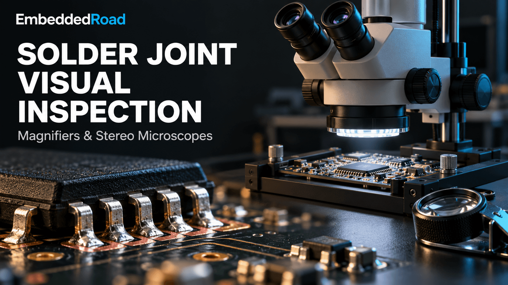
Visual inspection with magnifiers and stereo microscopes: magnification ranges, lighting setup, defect types caught, and when to escalate to X-ray.
Contents & prerequisites
Why Visual Inspection Matters in Solder Quality
Visual inspection remains the first and cheapest line of defense against solder defects, even in factories equipped with automated optical inspection (AOI) and X-ray inspection systems. A trained inspector with a magnifier or stereo microscope can catch problems that rule-based algorithms miss, especially novel defect modes that haven't been programmed into an AOI library yet. The cost of catching a defect here is measured in seconds of rework; the cost of missing it is a field return, a warranty claim, or in safety-critical products, a liability event.
Role of human-eye inspection in defect detection
Human pattern recognition is remarkably good at spotting "that doesn't look right" even when the deviation doesn't match a predefined rule. An experienced inspector recognizes dull, grainy solder before they can articulate why it's dull, and that intuition catches marginal wetting, flux residue patterns, and mechanical damage that automated systems tuned for geometric thresholds pass through cleanly. Visual inspection also serves as the calibration check for automated systems — when an AOI flags false positives or false negatives, a human at a microscope resolves the ambiguity.
Limitations of naked-eye assessment
The unaided human eye resolves roughly 0.1 mm to 0.2 mm at a comfortable 250 mm viewing distance, depending on contrast and lighting. Modern fine-pitch components — 0.4 mm pitch QFNs, 01005 passives, BGA balls under packages — fall below or near this threshold. Fatigue, inconsistent lighting, and operator-to-operator variability compound the problem. A defect visible to one inspector under raking light may be missed by another under flat illumination. This is why visual inspection needs optical magnification tools as standard equipment, not optional accessories, for any board built with components smaller than roughly 1.0 mm pitch.
Integration with automated inspection workflows
In a mature line, visual inspection isn't a replacement for AOI or X-ray — it's embedded between them. Operators perform first-article visual checks before a line is released to run, spot-check samples during production, and perform final disposition on parts that AOI flags as suspect. This triage role is where magnifiers and stereo microscopes earn their keep: they're fast enough to check a flagged joint in seconds, but detailed enough to make a confident accept/reject call without routing every ambiguous board to X-ray.
Hand Magnifiers: Selection and Practical Use
Magnification ranges and optical quality considerations
Hand magnifiers for solder work typically range from 2× to 10×. Below 4×, they add little over the naked eye for fine-pitch work; above 10×, hand tremor and the shrinking field of view make handheld use impractical. A 5× to 8× loupe with a multi-element achromatic lens is the practical sweet spot — single-element lenses introduce chromatic aberration and edge distortion that can hide or fake defects near the field periphery. Look for coated glass optics rather than molded plastic; plastic lenses scratch quickly in a production environment and degrade image quality within months.
Working distance and field of view trade-offs
Magnification and working distance trade off directly: a 10× loupe may only give 25 mm of clearance between lens and board, which is too tight for manipulating a hot iron or probe during rework verification. A 5× magnifier with 75–100 mm working distance leaves room to work while inspecting. Field of view shrinks proportionally with magnification too — at 10×, a typical loupe shows a circle of 15–20 mm diameter, enough for one connector or a handful of joints, not a whole board edge.
Ergonomic factors and inspection speed
Handheld magnifiers are fast for spot checks precisely because there's no setup: pick it up, look, put it down. For a technician spot-checking incoming reels or verifying a hand-soldered rework joint, this speed matters more than the modest resolution gain from a microscope. The trade-off is ergonomic — holding a loupe steady for extended periods causes hand and neck fatigue, and sustained close-focus work at awkward angles is a known contributor to repetitive strain. Headband-mounted magnifiers with flip-up lenses address some of this by freeing the hands, at some cost to optical stability.
Suitability for solder joint assessment
Hand magnifiers are appropriate for coarse-pitch through-hole and SMT work (0805 and larger, standard SOIC/QFP pitches), for first-pass triage, and for field or bench rework where a stereo microscope isn't available. They are not adequate as the primary inspection tool for BGA, QFN, or 0402/0201 passive placement — the magnification ceiling and lack of stable, controllable illumination make reliable defect calls difficult below roughly 0.5 mm feature size.
Stereo Microscopes: Setup and Technique
Binocular vs. trinocular configurations
Binocular stereo microscopes give the inspector two eyepieces and true stereoscopic depth perception, which is essential for judging solder fillet shape and joint height. Trinocular models add a third optical path for a camera, enabling simultaneous live viewing and image capture without removing an eyepiece. For any inspection station that needs documentation — which, per the discussion below, should be most of them — trinocular is worth the added cost over binocular-only.
Magnification selection (7×–50× range for soldering)
Soldering inspection generally lives in the 7× to 50× range. Zoom or step models covering roughly 7× to 45× handle the full span from whole-board overview to single-joint close-up without swapping objectives. Use 7×–10× for board-level overview and component placement checks, 20×–30× for standard SMT joint geometry assessment, and 40×–50× for fine-pitch BGA ball inspection or suspected hairline cracks. Magnification beyond 50× under a stereo microscope mostly produces a dim, shallow, shaky image with little added defect-detection value — that territory belongs to a metallurgical or digital microscope, not a stereo unit.
Illumination methods: coaxial, ring, and backlighting
Lighting setup determines whether real defects are visible or hidden in glare and shadow. Ring lights mounted around the objective give even, shadow-free illumination good for general survey work, but they can wash out subtle surface texture differences that distinguish a cold joint from a good one. Coaxial (through-the-lens) illumination reduces shadowing on reflective solder and is useful for reading markings or inspecting shiny BGA balls, but can produce hot-spot glare on curved fillets. Raking (low-angle, off-axis) light from a gooseneck or adjustable spot source is the single best tool for revealing wetting angle, surface graininess, and micro-cracks, because it throws shadows along surface irregularities that flat light conceals. Backlighting from beneath a translucent stage is useful for checking lead coplanarity and silhouette geometry against a component outline. A practical station combines a ring light for general work with one adjustable raking light for close defect confirmation.
Stage preparation and sample positioning
Boards should rest on a stable, vibration-damped stage with X-Y travel so the inspector can scan a row of joints without lifting and repositioning the board by hand, which reintroduces focus drift at high magnification. Anti-static mats and ESD-safe fixturing matter here as much as on the assembly line itself — an inspection station is still a point of ESD exposure for populated boards.
Depth of field and focus management
Depth of field shrinks sharply with magnification: at 10× it may be a few millimeters, at 40× it can be under 0.1 mm. On a board with components of varying height, this means refocusing between a tall connector and an adjacent low-profile resistor. Inspectors should learn to rock focus slightly through a joint rather than settling on one plane, since fillet defects like voids or disturbed solder often show up only when the focal plane passes through the joint's midsection.
Defect Detection: What to Look For
Solder joint geometry and wetting assessment
A good joint shows a concave fillet with a smooth, continuous transition from pad to lead, and a contact angle that indicates good wetting — generally well under 90° for eutectic SnPb or SAC alloys on a properly prepared pad. Convex, ball-shaped fillets with a high contact angle suggest poor wetting, often from inadequate flux activity, contamination, or an unsuitable reflow temperature profile.
Voiding, bridging, and cold solder identification
Surface voids are sometimes visible as small craters or pinholes in the fillet surface under raking light, though most voiding is subsurface and requires X-ray to quantify reliably. Bridging between adjacent leads is a straightforward visual catch at 10×–20×. Cold solder joints show a dull, grainy, or frosted surface texture instead of the smooth, bright surface of a properly reflowed joint — this is one of the clearest cases where raking illumination at 20×–30× outperforms flat ring lighting.
Pad cratering and component shift detection
Pad cratering — a crack in the laminate beneath the pad — is largely invisible optically unless it has progressed enough to show a visible fillet lift or pad tilt; cross-sectioning or acoustic microscopy is the definitive method. Component shift and tombstoning, by contrast, are easily confirmed visually against the original footprint outline at 7×–10× overview magnification.
IPC-A-600 visual acceptance criteria alignment
Solder joint and board surface acceptance should be judged against a documented standard rather than inspector judgment alone. IPC-A-610 covers acceptability of electronic assemblies, while the bare board itself should already have passed inspection against IPC-A-600 criteria at incoming inspection before it ever reached the line — a defect found post-assembly that traces back to a bare-board flaw (plating nodules, pad lifting, laminate voids) is a signal to tighten that earlier gate, not just rework the joint in front of you.
Documentation and Defect Recording
Photography through microscope eyepieces
Trinocular microscopes with a camera port produce the cleanest documentation, but even a phone camera held or clipped to a binocular eyepiece (afocal photography) can capture a usable record when no camera port exists. Lock exposure and white balance manually where possible — auto-exposure tends to blow out bright solder highlights and lose the texture detail that distinguishes cold joints from good ones.
Measurement techniques using reticles and graticules
An eyepiece reticle (a graticule with a calibrated scale) lets an inspector measure fillet height, void diameter, or lead-to-pad offset directly during inspection without a separate measurement step. Calibrate the reticle against a stage micrometer at each magnification setting used, since the scale's real-world value changes with zoom — a reticle division might represent 0.05 mm at 40× and 0.2 mm at 10×.
Traceability and defect log maintenance
Every defect call should be logged against a unique board or lot serial number, with defect type (using a standard code set, e.g., from IPC-A-610), location (reference designator and pin number), magnification used, and inspector initials. This log is what lets a quality team later correlate a field failure back to a specific reflow profile, paste lot, or shift — without it, a defect caught today teaches nothing about tomorrow's yield.
Image archiving for failure analysis
Captured images should be stored with the same board/lot identifier as the defect log entry, in a format and location that failure analysis can retrieve months later. A defect photo without a matching serial number and timestamp is nearly useless for root-cause work, since it can't be tied back to a specific process condition.
Limitations and When to Escalate
Subsurface defects beyond optical reach
No amount of magnification or lighting reveals what's under an opaque solder mass or beneath a BGA ball — voiding, head-in-pillow defects under a package body, and internal cracks require X-ray (2D or 3D CT) to assess. If a joint's exterior looks acceptable but the application is vibration- or thermal-cycling-sensitive, visual pass is not proof of internal integrity.
Transition from visual to instrumental inspection
A practical escalation rule: if a defect's existence or severity can't be confirmed by changing magnification or lighting angle within about 30 seconds, stop guessing and route the board to AOI re-scan or X-ray. Visual inspection is a screening and triage tool, not an arbiter for any defect where the acceptance criteria require a measurement optics can't make — void percentage, standoff height under an opaque package, or internal crack length.
Cost-benefit of manual screening vs. automated systems
A stereo microscope station costs a few thousand dollars and scales with trained labor hours; an AOI line scans every board at production speed but costs far more upfront and requires programming and maintenance. For low-volume or high-mix production, manual visual inspection at sampled intervals is often the more economical choice. For high-volume lines building safety- or mission-critical assemblies, 100% AOI coverage backed by sampled X-ray is the only approach that scales defect detection with throughput without proportionally scaling labor cost.
Human fatigue and inspection consistency challenges
Detection rates for trained inspectors measurably decline after sustained periods of repetitive fine-pitch inspection — this is a well-documented vigilance effect, not a reflection of operator skill. Rotating inspectors, limiting continuous microscope sessions, and using automated pre-screening to reduce the volume of boards requiring full manual review all help keep detection rates consistent across a shift rather than front-loaded into the first hour.
Learning
Sign in to track your progress.
Evidence
Public projects engineers linked to Visual Inspection: Magnifier and Stereo Microscope.
No engineer has linked a project to this topic yet. Built something that proves it? Add the project and tag it with soldering-visual-inspection-magnifier-and-stereo-microscope — it then shows here and on your public profile.