
Carrier Concentration: n and p in Thermal Equilibrium
Carrier concentration n and p in thermal equilibrium: intrinsic ni, doping, mass action law np=ni², Fermi level, and temperature effects.
Contents & prerequisites
What Is Thermal Equilibrium in Semiconductors?
Definition and physical meaning
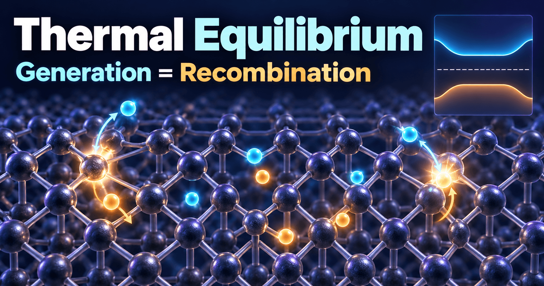
Thermal equilibrium is the condition where a semiconductor crystal sits at a uniform temperature with no external voltage, no light injection, and no net current flow, long enough that generation and recombination of carriers have balanced out. In this state, the electron concentration n and hole concentration p are stable, time-independent quantities set entirely by the material's bandgap, doping, and temperature. There is no external energy source pushing carriers around — every electron promoted to the conduction band by thermal energy is, on average, balanced by one falling back and recombining with a hole.
This is the baseline state every device model starts from. Before you can describe a diode turning on or a MOSFET channel inverting, you need the "resting" carrier populations that exist when nothing is being driven.
Why thermal equilibrium matters for device operation
Every compact model — the diode equation, the BJT Ebers-Moll model, the MOSFET drain current equations — is built by first establishing equilibrium carrier concentrations and then perturbing them with an applied bias. If you don't know n and p at equilibrium, you can't compute the built-in potential of a junction, the depletion width, or the saturation current. Equilibrium carrier concentration is the reference point from which all injection, extraction, and current-flow phenomena are measured.
Temperature dependence of carrier behavior
Carrier concentration in a semiconductor is fundamentally thermally activated. Electrons gain enough energy from lattice vibrations to jump the bandgap, and the population of carriers able to do this grows exponentially with temperature. This is why semiconductor behavior — unlike a resistor's relatively flat temperature coefficient — can change by orders of magnitude over an automotive or industrial temperature range, a point every reliability engineer eventually has to confront.
Intrinsic Carrier Concentration (ni)
Derivation from band structure and density of states
In a pure, undoped crystal — see Crystal Structure: Silicon Lattice and Covalent Bonds for the lattice picture — every electron in the conduction band leaves behind a hole in the valence band, so n = p = ni by definition. Using Fermi-Dirac statistics combined with the effective density of states in the conduction band (Nc) and valence band (Nv), the intrinsic concentration works out to:
ni = sqrt(Nc * Nv) * exp(-Eg / (2 * k * T))
where Eg is the bandgap energy, k is Boltzmann's constant, and T is absolute temperature. Nc and Nv themselves depend on the effective masses of electrons and holes and scale as T^(3/2).
Temperature scaling and exponential dependence on bandgap
The exponential term dominates. A small change in T produces a large change in ni because Eg/(2kT) sits in the exponent. This is also why different semiconductors behave so differently at the same temperature: germanium (Eg ≈ 0.66 eV) has a dramatically higher ni than silicon (Eg ≈ 1.12 eV) at room temperature, which is one of the practical reasons silicon displaced germanium for mainstream digital logic — lower intrinsic leakage.
Calculating ni for silicon and germanium
For silicon at T = 300 K, the commonly cited value is ni ≈ 1.0 × 10^10 cm^-3 (some references use 1.5 × 10^10 cm^-3 depending on the Nc/Nv values assumed — always check which constant your simulator or textbook uses before comparing numbers). For germanium at 300 K, ni is roughly three orders of magnitude higher, around 2.4 × 10^13 cm^-3. When you need a precise value for a design calculation, pull it from the device simulator's material file or a current semiconductor physics reference rather than from memory, since published constants (Nc, Nv, Eg) vary slightly between sources.
Impact on undoped semiconductor properties
Because ni is so small for silicon, undoped ("intrinsic") silicon is a poor conductor at room temperature — conductivity scales with carrier concentration, and 10^10 cm^-3 is minuscule next to the ~5 × 10^22 cm^-3 atomic density of the silicon lattice itself. This is precisely why doping is necessary to make silicon useful: intrinsic material alone cannot supply enough carriers for practical device currents.
Doped Semiconductors: Majority and Minority Carriers
Electron concentration (n) in n-type material
Adding donor impurities (phosphorus, arsenic) contributes free electrons without corresponding holes. At room temperature, essentially all shallow donors are ionized, so n ≈ Nd, the donor concentration, provided Nd >> ni. Electrons become the majority carrier.
Hole concentration (p) in p-type material
Adding acceptor impurities (boron) contributes holes. Similarly, p ≈ Na, the acceptor concentration, when Na >> ni, and holes are the majority carrier. The mechanism of substituting dopant atoms into the lattice and the energy levels they introduce is covered in detail in Donor (n-type) and Acceptor (p-type) Impurity Doping.
Dopant ionization and compensation effects
Real wafers often contain both donor and acceptor atoms in the same region (from sequential implant steps). The net doping is Nd − Na (or Na − Nd), and this compensation determines whether the region behaves as n-type or p-type. Full ionization is a good approximation at room temperature for shallow dopants in silicon, but it breaks down at cryogenic temperatures, discussed below under freeze-out.
Relationship between doping level and carrier concentration
For typical doping levels used in CMOS processes — roughly 10^15 to 10^20 cm^-3 — majority carrier concentration tracks the net dopant density almost linearly, while the minority carrier concentration collapses according to the mass action law.
The Mass Action Law and np Product
Fundamental equilibrium relation: np = ni²
In thermal equilibrium, regardless of doping, the product of electron and hole concentrations is fixed at a given temperature:
n * p = ni^2
Why the product remains constant at fixed temperature
This relation falls directly out of equating the generation rate (thermal excitation across the bandgap, independent of doping) with the recombination rate (proportional to n*p). At equilibrium these rates match, and since generation rate depends only on T and Eg, the np product is pinned to ni², which is itself only a function of T.
Applying mass action law to n-type and p-type regions
Worked example: an n-type silicon region doped at Nd = 1 × 10^16 cm^-3, with ni = 1.0 × 10^10 cm^-3 at 300 K.
n ≈ Nd = 1e16 cm^-3
p = ni^2 / n = (1e10)^2 / 1e16 = 1e4 cm^-3
The minority hole concentration is 12 orders of magnitude smaller than the majority electron concentration — a ratio that explains why minority carrier currents are so sensitive to small perturbations like injection at a forward-biased junction.
Implications for forward and reverse bias operation
This equilibrium np = ni² relationship is the quiet backbone of diode behavior. Forward bias injects excess minority carriers and pushes np above ni², driving the exponential current described in Forward Bias: Exponential Current, Knee Voltage. Reverse bias instead depletes carriers near the junction, pulling np below ni² locally and producing the small leakage currents analyzed in Reverse Bias: Leakage Current, Breakdown Mechanisms.
Fermi Level Position and Carrier Distribution
Fermi-Dirac statistics in thermal equilibrium
The Fermi level EF is the energy at which the probability of occupation by an electron is exactly 50% in equilibrium. Carrier concentrations follow directly from EF's position relative to the conduction and valence band edges, using Fermi-Dirac statistics (or its Boltzmann approximation for non-degenerate semiconductors).
How doping shifts the Fermi level within the bandgap
In intrinsic silicon, EF sits near mid-gap. Donor doping pulls EF up toward the conduction band edge; acceptor doping pulls it down toward the valence band edge. The further EF moves from mid-gap, the larger the majority-to-minority carrier ratio.
Calculating carrier concentrations from Fermi level position
The standard relations are:
n = Nc * exp(-(Ec - EF) / (k*T))
p = Nv * exp(-(EF - Ev) / (k*T))
Multiplying these two confirms np = NcNvexp(-Eg/kT) = ni², independent of where EF actually sits — a useful consistency check when debugging a TCAD setup.
Distinction between quasi-Fermi levels under bias
Once a device is biased, n and p are no longer tied to a single EF — each carrier type gets its own quasi-Fermi level (Fn and Fp), and their separation quantifies how far the device has been pushed from equilibrium. That splitting is what lets forward-biased junctions sustain np >> ni² locally without violating any physical law; equilibrium mass-action law simply no longer applies region-by-region.
Temperature Effects on n and p
Intrinsic carrier growth with temperature
Because ni grows exponentially with T, at sufficiently high temperature ni can exceed the doping concentration, and the material behaves as if it were intrinsic again — carrier concentration becomes temperature-dominated rather than dopant-dominated.
Freeze-out and saturation regimes in doped material
At low temperature, dopants don't have enough thermal energy to ionize, so n or p drops well below Nd or Na — this is carrier freeze-out, a real concern for cryogenic CMOS. In the middle range (roughly 150 K to 450 K for typical silicon doping), carrier concentration is flat and dopant-controlled — the "saturation" region where most devices are designed to operate.
Practical temperature range for stable carrier concentration
For a design, confirm the saturation range for your specific doping level and process by consulting the process technology file or TCAD material deck — the exact boundaries shift with doping concentration.
Leakage current implications at elevated temperatures
As junction temperature rises toward the point where ni approaches the doping level, reverse leakage current — already proportional to ni² in the depletion region — grows rapidly, which is why datasheets specify leakage at multiple temperatures and why thermal design margin matters for reverse-biased junctions.
Equilibrium vs. Non-Equilibrium: Setting the Stage
When thermal equilibrium assumptions hold
Thermal equilibrium strictly applies only with zero applied bias and no illumination. It remains an excellent approximation deep inside quasi-neutral regions of a biased device, away from junctions, which is why the Depletion Approximation and Charge Neutrality framework can still borrow equilibrium carrier relations outside the depletion region.
Transition to quasi-equilibrium under applied bias
Under moderate bias, carrier populations shift but can often still be described locally with quasi-Fermi levels — this is the quasi-equilibrium approximation used throughout standard diode and transistor models.
Carrier injection and extraction mechanisms
Forward bias injects minority carriers across a junction; reverse bias extracts them, leaving the depletion region nearly carrier-free. Both processes are deviations from — and are quantitatively measured against — the equilibrium np = ni² baseline established in this article.
Connection to forward and reverse bias regimes
Everything in the next tier of this series — junction built-in potential, depletion width, diode I-V behavior — is a perturbation analysis layered on top of the equilibrium carrier concentrations covered here.
Learning
Sign in to track your progress.
Evidence
Public projects engineers linked to Carrier Concentration: n and p in Thermal Equilibrium.
No engineer has linked a project to this topic yet. Built something that proves it? Add the project and tag it with vlsi-semiconductor-carrier-concentration-n-and-p-in-thermal-equilibri — it then shows here and on your public profile.