
Battery Management: Charge Path, Protection FET Layout
Protection FET layout guidance covering charge-path routing, gate-drive design, thermal management, and EMI control beyond datasheet specs.
Contents & prerequisites
Why Protection FET Placement Matters
Role of protection FETs in battery circuits
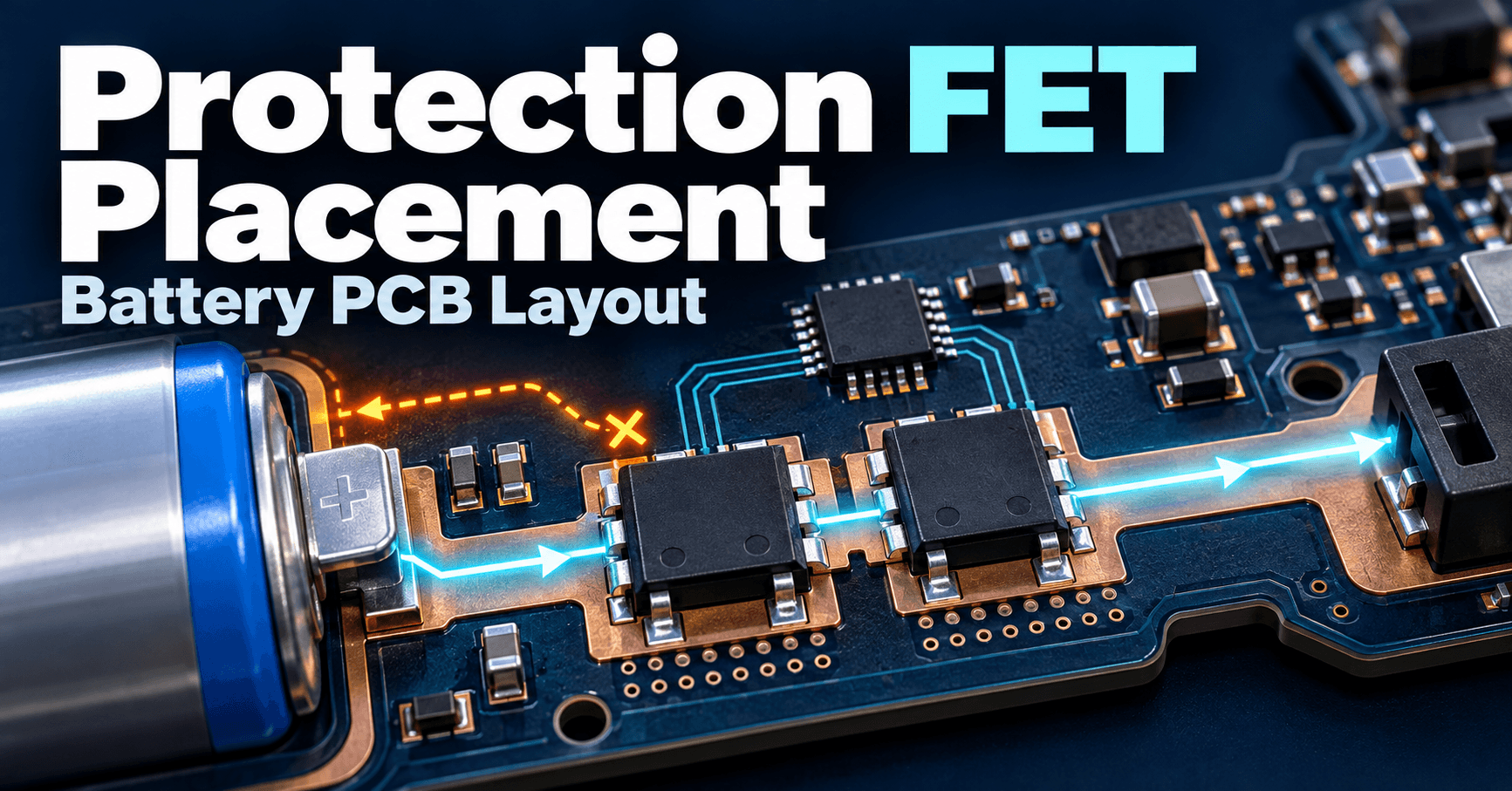
Protection FETs sit in the charge and discharge current path of a battery pack, typically as back-to-back N-channel MOSFETs controlled by a protection IC or fuel-gauge/protector combo. Their job is binary but critical: disconnect the battery from the system during overcurrent, overvoltage, undervoltage, or overtemperature events. Unlike a charger IC's switching FETs, which operate continuously at high frequency, protection FETs spend most of their life fully on (low RDS(on), minimal switching) and occasionally slam fully off under fault conditions. That duty cycle shapes every layout decision that follows — the design has to be optimized for low conduction loss during normal operation and for surviving a hard, fast turn-off during a fault.
Thermal and current-distribution concerns
At continuous charge/discharge currents of several amps, even a FET with RDS(on) of a few milliohms dissipates real power: P = I²R. At 10 A through 5 mΩ, that's 500 mW per FET, concentrated in a package that's often a few square millimeters. Without a deliberate thermal path, junction temperature rises until RDS(on) increases further, which raises dissipation further — a positive feedback loop that ends in thermal shutdown or FET degradation. Current distribution matters just as much as total dissipation: if copper pours funnel current unevenly through a dual-FET package, one die runs hotter than the other even though the datasheet assumes symmetric current sharing.
Cost of poor placement: EMI and efficiency loss
A protection FET placed far from the battery terminals, or routed with long, thin traces to save board space, adds resistance and inductance to the charge path. Resistance shows up directly as I²R loss and voltage droop under load. Inductance is worse: every fast current transition (a fault-triggered turn-off, a load step, a connector hot-plug) interacts with that parasitic inductance to produce V = L(di/dt) spikes that can exceed the FET's voltage rating or radiate as broadband EMI. A layout that looks fine on a DC continuity check can still fail EMC testing or damage a FET during a load dump, purely because of trace geometry.
Charge-Path Current Flow & PCB Routing
Identifying the primary charge path from connector to battery
Before placing a single component, trace the actual current path on paper: input connector → charger IC power stage → protection FET(s) → battery terminals, and the mirror path for discharge into the system load. This path should be the widest, shortest, most direct copper on the board — not squeezed around decoupling capacitors or digital routing. The protection FET belongs physically close to the battery terminals, not the charger IC, for a specific reason: the FET must interrupt all current paths between the battery and the rest of the system, including the load path that bypasses the charger IC entirely during discharge. Placing it near the charger instead leaves a segment of PCB copper between the battery and the disconnect point permanently energized, which defeats the protection function during a short circuit on that segment and adds unprotected trace length that a fault current must still flow through before disconnection takes effect.
Minimizing loop area to reduce di/dt noise
The current loop formed by battery positive → protection FET → return path → battery negative should be as physically tight as possible. Large loop area is an effective antenna for both emitted EMI and susceptibility to external fields. Route the forward and return conductors on adjacent layers, directly overlapping, rather than on the same layer separated by routing for other nets.
Star-point grounding for charge-return paths
Charge-return current, protection circuitry ground, and sensitive analog grounds (coulomb counter, thermistor reference) should not share a common trace segment. Use a single star point where the high-current return path ties into the ground plane, physically separated from where low-current analog references tie in, so that I×R drop from charge current doesn't modulate the analog ground reference.
Kelvin sensing and current-sense resistor placement
If the protection IC uses an external current-sense resistor, the sense traces must be routed as a true Kelvin pair — connecting directly to the resistor pads, not to the power traces feeding the resistor. Tapping sense lines from the wrong side of a via or pad introduces the via's resistance into the measurement, which on a 2 mΩ sense resistor can be a double-digit percentage error.
Protection FET Gate-Drive Layout
Gate-drive signal integrity and switching speed
Even though protection FETs switch rarely, when they do switch, they switch fast and under worst-case conditions (fault current, not nominal load). The gate driver sees a lower effective impedance path demand during this edge, and any resistance or inductance in the gate loop slows the turn-off — exactly when fast turn-off is most needed to limit fault energy.
Separating gate traces from power-delivery paths
Gate traces should run away from the high-current power plane, ideally on a different layer with ground shielding between them. Capacitive coupling from a switching drain node into an adjacent gate trace can cause false turn-on or ringing, particularly during the fast dV/dt of a fault-triggered disconnect.
Pull-down resistor placement and thermal considerations
The gate pull-down (or pull-up, for the protection IC's internal driver) should sit as close to the FET gate pin as physically possible, minimizing the loop between driver output, resistor, and gate. This loop inductance directly affects switching performance: higher gate-loop inductance slows both turn-on and turn-off edges, increases ringing on the gate waveform, and can push the FET into its linear region for longer during a fault, increasing instantaneous power dissipation well beyond the steady-state rating.
Bootstrap capacitor location for high-side FETs
For high-side protection FET configurations requiring a bootstrap or charge-pump supply, the bootstrap capacitor must sit immediately adjacent to the driver's bootstrap pins — the same close-to-IC principle covered in Capacitor Placement Rules: Closest to IC Power Pin. A long bootstrap trace adds inductance that degrades the gate drive voltage available during turn-on, particularly under the high dI/dt of a fault event.
Thermal Management & Current Distribution
Heat dissipation in series and parallel FET configurations
Back-to-back series FETs (common/common-drain configuration) each carry the full pack current, so total conduction loss is additive across both devices. Paralleled FETs split current, but only if their RDS(on) and thermal paths are matched; a 10% RDS(on) mismatch between two paralleled dies translates to meaningfully unequal current sharing and therefore unequal heating.
Via stitching and copper plane connectivity
Thermal vias under and around the FET's exposed pad, stitched to an internal or bottom copper pour, are the primary heat-extraction path. Follow the pad's annular ring and hole-size guidance the same way you would for any plated via — see Annular Ring: IPC-6012 Minimum Ring Requirement — since undersized rings or inadequate hole fill reduce the thermal and electrical conductivity of the via array.
Paralleling protection FETs for load sharing
When paralleling FETs for higher current capacity, keep gate traces length-matched and symmetric, and lay out the drain/source copper so each FET sees an equal-length, equal-width path to the shared node. Asymmetric copper causes one FET to turn on microseconds before the other, briefly carrying the full current alone.
Thermal simulation and derating guidelines
Use the FET manufacturer's thermal resistance curves (RθJA, RθJC) combined with your actual copper area in a simulation or spreadsheet calculation, rather than relying on the datasheet's test-board assumptions, which typically use far more copper than a compact battery pack board allows. Derate accordingly — many designers target 70-80% of the datasheet's continuous current rating as a practical ceiling for a space-constrained layout.
Decoupling & Power Integrity Near FET Switching
Local bypass capacitors for FET switching noise
Even in a protection circuit, the fast edges during fault turn-off generate high-frequency noise that benefits from local decoupling at the charger IC and protection IC supply pins. This reduces the EMI radiated by the switching event and stabilizes the IC's internal reference during the transient.
ESR and ESL effects on transient voltage spikes
The capacitor's parasitic ESR and ESL determine how effectively it suppresses a fast spike versus a slower ripple component; a capacitor with low ESL responds to the nanosecond-scale edges typical of FET switching, while bulk capacitance with higher ESR handles lower-frequency ripple. The frequency-dependent behavior is covered in detail in Capacitor ESR and ESL: Impedance Profile vs. Frequency, and it's directly applicable here: a single bulk capacitor placed far from the FET will not suppress the spike a small, close-placed ceramic would.
Placement relative to FET source/drain pins
Place the bypass capacitor directly across the FET's drain-source or across the supply rail immediately adjacent to the switching node, not several millimeters away connected by a thin trace — that trace's inductance undermines the capacitor's high-frequency effectiveness regardless of its rated ESL.
Interaction with charger IC power pins
The charger IC's input and output decoupling should follow the same close-to-pin discipline, and should not share a via or copper pour segment with the protection FET's switching node, to avoid injecting switching noise into the charger's control loop.
Common Layout Mistakes & Mitigation
Gate trace coupling to power and signal lines
Routing a gate trace parallel and adjacent to a power trace for even a few millimeters creates a coupling path that can turn a clean gate signal into one riddled with switching-induced glitches. Mitigate with a ground-plane layer between them or physical separation.
Inadequate vias and thermal connections
A single via under a FET's thermal pad is rarely sufficient for currents above a couple of amps; use an array sized to the current and power dissipation, following the same rigor used for any high-current thermal via field.
Asymmetric charge and discharge paths
Charge and discharge current often flow through different sense or FET arrangements (particularly in designs with independent charge/discharge FETs). These paths should be reviewed separately for resistance and inductance — an efficient discharge path paired with a resistive charge path produces asymmetric efficiency and thermal behavior that isn't obvious from a single-direction test.
Floating grounds between protection and charger circuits
If the protection IC's ground and the charger IC's ground connect only through a long, narrow trace or through the battery connector itself, transient currents during a fault can produce ground bounce that destabilizes both ICs simultaneously. Tie grounds together at a single low-impedance point near the battery connector.
Design Verification & Measurement
Thermal imaging during charge cycles
Run the pack through a full charge cycle at rated current with a thermal camera on the protection FETs. Look for hot spots that don't match the expected symmetric pattern — these indicate current imbalance in paralleled FETs or poor via thermal connectivity.
Oscilloscope probe placement for switching transients
Probe directly across the FET's drain-source pins with the shortest possible ground lead (a scope probe's ground clip lead adds inductance that will ring and mask the real signal) to capture genuine turn-off spikes rather than probe-induced artifacts.
IR drop measurement across battery path
Measure voltage drop from battery terminal to system load terminal at full load current using a 4-wire (Kelvin) measurement; this reveals the actual resistance contributed by FET RDS(on), copper, and connectors combined, separate from the datasheet's per-component numbers.
Validation of gate-drive timing and slew rate
Confirm gate turn-off time and resulting drain voltage overshoot against the FET's absolute maximum VDS rating under worst-case fault current, not just nominal load current — this is where gate-loop inductance and layout parasitics most often produce a rating violation that a nominal-current test would miss. Also check the reverse-bias behavior of the body diode during the dead-time between FET states, since reverse recovery and leakage characteristics documented in Reverse Bias: Leakage Current, Breakdown Mechanisms directly affect how much voltage the FET must block during that interval.
Learning
Sign in to track your progress.
Evidence
Public projects engineers linked to Battery Management: Charge Path, Protection FET Layout.
No engineer has linked a project to this topic yet. Built something that proves it? Add the project and tag it with pcb-and-battery-management-charge-path-protection-fet-layo — it then shows here and on your public profile.