
Temperature Compensation: CTAT and PTAT
Learn how CTAT and PTAT circuits cancel temperature drift in analog ICs, with worked PTAT current derivation and bandgap design trade-offs.
Contents & prerequisites
Prerequisites
Why Temperature Compensation Matters
Device performance drift across temperature ranges
Every semiconductor parameter you depend on moves with temperature. Threshold voltage drops roughly 1-2 mV/°C in a typical CMOS process. Carrier mobility falls as temperature rises, cutting transistor transconductance. Diode and BJT forward voltages drop by about 1.5-2.2 mV/°C. None of these drifts are optional extras you can design around once and forget — they are baked into the silicon lattice itself, a consequence of how carrier concentration and bandgap energy behave as described by Crystal Structure: Silicon Lattice and Covalent Bonds. A chip that works at 27°C on the bench can show 5-10% parameter shifts by the time it reaches 125°C junction temperature in the field.
Impact on analog circuit accuracy and reliability
Uncompensated drift shows up as gain error in instrumentation amplifiers, offset walk in comparators, and frequency drift in oscillators. A bias current that changes by 20% over the automotive temperature range (-40°C to 125°C) will shift the quiescent point of every stage downstream of it. In ADC and DAC front ends, reference drift directly translates to code error — a 1% reference shift can burn an entire bit of resolution in a 10-bit converter. Reliability margins (electromigration, hot-carrier aging) are also temperature-dependent, so a circuit that silently drifts out of spec at temperature may also be aging faster than the datasheet assumes.
Real-world constraints in VLSI design
You cannot just throw calibration at the problem — trim bits, fuses, and digital correction cost test time and die area, and one-time trim at 25°C doesn't fix a non-flat temperature curve. The economical answer is to build temperature independence into the analog core itself, using devices whose drifts are well characterized and predictable, then cancel one drift against another. That is exactly what CTAT (complementary-to-absolute-temperature) and PTAT (proportional-to-absolute-temperature) circuits do, and they are the foundation block underneath every bandgap reference you will design later.
PTAT Circuits: Proportional-to-Absolute-Temperature
Physical basis: thermal voltage and exponential current behavior
The thermal voltage V_T = kT/q sits at the center of PTAT behavior. At room temperature it's about 25.85 mV, and it scales linearly with absolute temperature — a clean, predictable, physics-guaranteed slope of roughly 0.0862 mV/K. Any circuit that produces an output voltage or current proportional to V_T inherits that linear, positive temperature coefficient. The underlying mechanism is the diode/BJT exponential I-V relationship, the same exponential law covered in Forward Bias: Exponential Current, Knee Voltage: I = I_S(e^(V/V_T) - 1). Take the difference between two diode voltages running at different current densities, and the exponential term cancels, leaving a term directly proportional to V_T.
Circuit implementation using matched diodes and resistors
The classic implementation uses two matched bipolar devices (diode-connected BJTs are preferred over plain diodes because of their superior ideality factor and better matching) biased at different current densities, usually through an area ratio N. The difference in their base-emitter voltages is:
ΔV_BE = V_T · ln(N)
This ΔV_BE is forced across a resistor to generate a current:
I_PTAT = ΔV_BE / R = (V_T · ln(N)) / R
Because V_T is linear in T and ln(N) and R are (to first order) temperature-independent, I_PTAT comes out linear in absolute temperature.
Deriving linear PTAT current from bipolar transistors
Worked example: two BJTs, Q1 at unit emitter area and Q2 at 8× area (N = 8), both biased by a current mirror so their collector currents are forced equal. At T = 300 K, V_T ≈ 25.85 mV, ln(8) ≈ 2.079, so ΔV_BE ≈ 53.7 mV. With R = 10 kΩ, I_PTAT ≈ 5.37 µA. At T = 358 K (85°C), V_T scales to about 30.86 mV, giving ΔV_BE ≈ 64.2 mV and I_PTAT ≈ 6.42 µA — a 19.5% increase over a 58°C rise, consistent with the ~0.33%/°C slope characteristic of PTAT cells. The matched current condition is normally enforced with a simple current mirror; the resistor ratio and the area ratio N are the two parameters you tune at the schematic level, and the resistor's own temperature coefficient (from Voltage Divider and Current Divider Rules territory when you're splitting currents across mirror branches) needs to be accounted for separately or it will distort the slope.
Scaling and design trade-offs
Larger N gives a larger ΔV_BE and better immunity to offset and mismatch, but costs more silicon area for the larger device. Practical area ratios run from 4:1 to 24:1; beyond that, returns diminish and parasitic effects (base resistance, non-ideal injection) start to matter. R's absolute value sets the current magnitude — smaller R means higher current, faster transient response, and more power, while larger R saves power but makes the circuit more sensitive to leakage currents and amplifier offset in the loop that forces the matched-current condition.
CTAT Circuits: Complementary-to-Absolute-Temperature
Negative temperature coefficient sources and mechanisms
CTAT behavior arises because the saturation current I_S of a p-n junction rises exponentially with temperature (through the bandgap-dependent term in the Shockley equation), far outpacing the linear rise in V_T. For a fixed forward current, the net effect is that V_BE must decrease as temperature rises to keep I = I_S·e^(V_BE/V_T) constant.
Base-emitter voltage as a CTAT reference
V_BE at constant current is the standard CTAT reference. Its temperature coefficient is typically -1.5 mV/°C to -2.2 mV/°C depending on process and bias current, and it's reasonably linear over a moderate range, though it bends at temperature extremes due to the bandgap's own weak temperature dependence.
Achieving steep negative slope for precise cancellation
The slope magnitude depends on bias current density: lower current density gives a slightly steeper negative slope but also a lower absolute V_BE, which changes the headroom available in the summing network. Designers choose bias current to balance slope requirements against the output swing needed by the following stage, often a current mirror or Two-Stage Op-Amp: Differential Input + Common-Source Output acting as the summing amplifier.
Practical implementation constraints
V_BE's absolute value and slope both depend on process spread — a slow process corner can shift V_BE by tens of millivolts. This is why CTAT alone is never trimmed in isolation; it is always calibrated as part of the full compensated reference, not as a standalone block.
Combining CTAT and PTAT: The Compensation Strategy
Principle of cancellation: opposing temperature coefficients
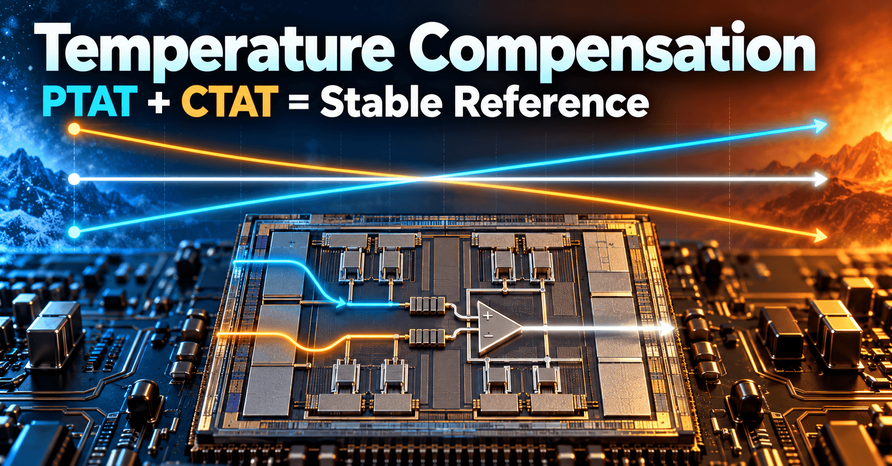
The core idea: V_BE falls with temperature, ΔV_BE (and thus I_PTAT) rises with temperature. Scale and sum them so the slopes cancel:
V_REF = V_BE + K · ΔV_BE
Choosing K ≈ 17-18 in a typical silicon process makes the composite roughly flat near room temperature — the classic 1.2 V bandgap result.
Weighted summation and tuning for flatness
K is implemented as a resistor ratio, so the whole reference reduces to matching resistors and area ratios precisely — both of which are far better controlled across process and temperature than absolute device parameters.
First-order and higher-order temperature compensation
First-order cancellation (linear terms only) typically achieves 20-50 ppm/°C. Residual curvature comes from V_BE's own non-linear temperature dependence. Higher-order compensation adds correction terms (often a V_T·ln(T) term) to flatten the curve further, pushing performance toward single-digit ppm/°C, at the cost of extra circuitry and calibration complexity.
Trade-off between accuracy and silicon area
Every added correction order brings more devices, more matching requirements, and more test/trim time. Most commercial designs stop at first- or second-order compensation unless the application (precision instrumentation, metrology) specifically demands better.
Applications in On-Chip References and Biasing
Temperature-stable bias currents for analog blocks
PTAT and CTAT currents, summed in the right ratio, create bias currents with near-zero temperature coefficient, used to bias amplifier tail currents, comparator references, and oscillator cores.
Integration with bandgap reference circuits
The bandgap reference is the canonical consumer of this technique — it is literally a CTAT V_BE plus a scaled PTAT ΔV_BE, summed at a high-impedance node.
Compensation in op-amp tail currents and gain stages
A PTAT-biased tail current compensates for the mobility degradation that reduces transconductance at high temperature, keeping gain-bandwidth more stable across the full range.
Cascaded compensation for multi-stage systems
In multi-stage designs, each stage may need its own local compensation network tuned to its own dominant drift mechanism, then referenced back to a single master bandgap for consistency.
Layout, Matching, and Practical Considerations
Device mismatch effects on CTAT/PTAT accuracy
Random mismatch in V_BE between "matched" devices directly appears as reference error — a 1 mV mismatch can translate to several mV of bandgap error depending on the summation gain K.
Thermal gradient management on die
Place PTAT-generating pairs close together, use common-centroid layout, and keep them away from high-power blocks that create local hot spots, since a gradient across the die defeats the assumption that both devices see the same T.
Process corner variations and robustness
Simulate across all process corners, not just typical — β variation, resistor TC spread, and I_S variation all interact with the compensation ratio K.
Measurement and characterization techniques
Characterize across a temperature chamber sweep at multiple supply voltages, plotting ppm/°C against trim code to find the real inflection point, not just the simulated one.
Design Trade-offs and Optimization
Power consumption versus compensation order
Higher-order compensation and additional correction amplifiers cost quiescent current; low-power designs often accept 30-50 ppm/°C to save microamps.
Temperature range coverage and curvature
Automotive and industrial ranges (-40°C to 125°C or 150°C) show more curvature than consumer ranges (0°C to 70°C), demanding higher-order correction for the same ppm/°C spec.
Integration with power management and dynamic scaling
References shared with DVFS or power-gated domains must settle quickly after wake-up, so bias currents and compensation networks need fast startup, not just steady-state accuracy.
Verification and post-silicon tuning
Budget trim bits for K and for absolute output level separately — curvature correction and offset correction are largely independent and should not be tuned together.
Learning
Sign in to track your progress.
Evidence
Public projects engineers linked to Temperature Compensation: CTAT and PTAT.
No engineer has linked a project to this topic yet. Built something that proves it? Add the project and tag it with vlsi-chip-temperature-compensation-ctat-and-ptat — it then shows here and on your public profile.