
Drive Strength: X1, X2, X4, X8, X16 Cell Variants
Drive strength X1 through X16 cell variants explained: how transistor sizing scales timing, slew, fanout, area, and leakage in standard cell libraries.
Contents & prerequisites
What is Drive Strength and Why It Matters
Definition: transistor sizing and output current capability
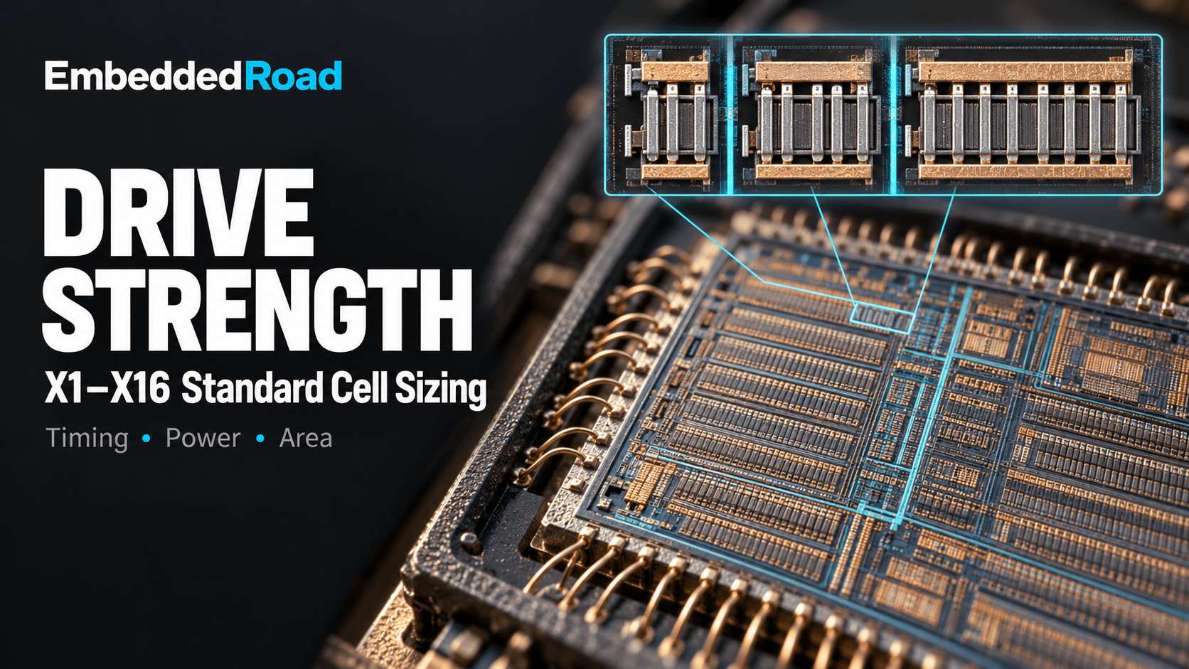
Drive strength describes how much output current a standard cell can source or sink, and in practice it's implemented by scaling the width of the pull-up and pull-down transistors inside the cell while holding the channel length fixed at the process minimum. A buffer cell named BUF_X4 is electrically the same logic function as BUF_X1, but its NMOS and PMOS devices are roughly four times wider, giving it roughly four times the saturation current and therefore the ability to charge and discharge a load capacitor four times faster for a given input slew. The X multiplier in the cell name is not an arbitrary marketing label — it's a direct, library-defined ratio against the unit cell's drive current, and that ratio is what a synthesis or STA tool reads when it decides whether a cell can meet a timing requirement.
Role in timing closure and power budgeting
Every combinational path in a design is a chain of gate delays plus wire delays, and gate delay is dominated by how quickly a cell can drive its output node to the switching threshold. Drive strength is the knob that trades silicon area and power for speed on a cell-by-cell basis. A synthesis tool doesn't pick the fastest cell everywhere — that would blow the power and area budget — it picks the smallest cell that still meets the timing constraint on each path, which means an experienced engineer needs to understand why a X8 inverter shows up on one net and a X1 shows up two gates later.
Impact on slew rate, delay, and fanout
Three things move together whenever drive strength changes: the cell's own propagation delay drops as strength increases (for a fixed load), the output transition time (slew) improves because more current charges the load faster, and the maximum fanout the cell can safely drive goes up because a stronger driver can absorb more downstream input capacitance without its output slew degrading past the library's transition-time limit. These three are read out of the same lookup tables in timing analysis, so a single library characterization run captures all of them simultaneously.
The X1 Base Cell: Standard Reference
X1 as the unit cell definition
The X1 cell in a standard cell library is the normalization reference — by convention its drive current, area, and input capacitance are treated as "1 unit" and every other variant (X2, X4, X8, X16, and sometimes oddball ratios like X1.5 or X6) is expressed as a multiple of it. This is a library-specific convention: an X1 inverter in one foundry's 28 nm library and an X1 inverter in another vendor's 16 nm library have no fixed relationship to each other. The X-number is only meaningful for comparing cells within the same library family.
Minimum transistor dimensions and W/L ratios
At the transistor level, the X1 cell uses close to the minimum allowed channel width for the process node, subject to the PMOS-to-NMOS width ratio needed to balance rise and fall drive (since hole mobility is lower than electron mobility, PMOS devices are typically drawn 1.5–2.5x wider than NMOS in a balanced inverter, with the exact ratio set during characterization). The channel length is held at the process-defined minimum (or a slightly relaxed "nominal" length used throughout the digital library) across every drive strength variant — length scaling is not how strength is varied in digital standard cells, width is.
Baseline propagation delay and output capacitance
The X1 cell's propagation delay at zero or minimal output load, and its input pin capacitance, become the two baseline numbers against which every other variant is judged. A designer reading a .lib file should expect the X1 inverter's intrinsic delay to be the largest among the family (because it has the least drive current), and its input capacitance to be the smallest (because its gates are the narrowest) — both of these invert as you move up the X-scale.
Scaling Logic: X2, X4, X8, X16 Progression
Proportional transistor upsizing methodology
In an idealized library, X2 is built by doubling the gate width of every transistor in the X1 schematic, X4 quadruples it, and so on, keeping the W/L ratios between NMOS and PMOS identical so switching behavior and noise margins stay consistent across the family. In practice, foundry libraries deviate from perfect doubling for layout and DRC reasons — fin-count quantization in FinFET processes means a X4 cell might use 4x the fins of X1, but X3 (if it exists) might round to the nearest achievable fin count rather than landing exactly on 3x current.
Drive current scaling and relationship to multiplier
Drive current in the saturation region scales roughly linearly with transistor width for a fixed length and fixed gate overdrive, so a X8 cell's saturation current should be close to 8x that of X1. This is an approximation, not an exact law — velocity saturation, short-channel effects, and self-heating all bend the relationship away from strict linearity at advanced nodes, which is exactly why SPICE characterization rather than hand calculation is used to generate the final library numbers (more on this later in the article).
Delay reduction vs. area and power trade-offs
The practical consequence: going from X1 to X2 for a given load typically cuts intrinsic delay close to 2x, but going from X8 to X16 yields a smaller fractional improvement once the external wire and fanout capacitance (not the internal gate capacitance) dominates total delay. This diminishing return is the central trade-off an engineer must recognize — doubling drive strength repeatedly does not keep buying proportional speed once you're load-dominated rather than drive-dominated, but it keeps costing area and leakage every time.
Timing and Electrical Characteristics
Propagation delay curves across drive strengths
A standard-cell delay model (captured in the .lib file as a nonlinear delay model, NLDM, table or a current-source model, CCS/ECSM) is indexed by input transition and output load. For a fixed load, plotting delay against drive strength across X1 through X16 produces a curve that drops steeply at first and flattens — the classic 1/x shape — because delay is proportional to load capacitance divided by drive current, and drive current is what's scaling.
Output slew rate improvement with larger cells
Output slew (the 10%–90% or 20%–80% transition time) improves with drive strength for the same reason delay does, and in most libraries slew improvement is the more operationally important number because slew violations trigger DRC-style transition checks independent of whether the path timing is met.
Transition time and rise/fall asymmetry
Because NMOS and PMOS mobility differs, rise and fall delays are rarely equal even in a "balanced" cell, and this asymmetry persists across the X-family — it does not cancel out by upsizing. Designers chasing a tight setup margin on a rising edge specifically need to check the rise-delay column of the library table, not just the nominal or average delay.
Maximum fanout specifications per variant
Libraries publish a max_capacitance (or max_fanout) attribute per cell that caps how much load a given drive strength is allowed to drive while staying within a slew limit — exceeding it is flagged as a DRC violation in STA even if the delay number is technically computable. A X1 buffer might be rated for a handful of minimum-size inputs, while a X16 buffer might be rated to drive a long clock-like net or dozens of fanout pins; the exact numbers must come from the specific library's datasheet, not estimation.
Area, Power, and Leakage Considerations
Chip area increase with drive strength multiplier
Cell area scales with transistor width, so a X16 inverter occupies noticeably more placement area than a X1 — not usually a full 16x in area because of fixed overhead (well spacing, contacts, and poly pitch don't shrink), but area growth per step is substantial and linear-ish in the active region. In area-constrained blocks, blanket upsizing for timing margin is a quick way to blow a utilization target.
Dynamic power consumption scaling
Dynamic power is proportional to C·V²·f, and a larger drive-strength cell has more internal (self) capacitance, so its switching power per toggle increases with its size even before counting what it's driving. This is the direct power cost of the delay improvement — there's no free lunch between X1 and X16.
Static leakage current trends in larger cells
Leakage scales close to linearly with transistor width as well, since more parallel fingers means more subthreshold leakage paths. A X16 cell can leak on the order of an order of magnitude more than an X1 cell of the same function, which matters enormously in sleep-mode or standby power budgets — always check the leakage_power group in the .lib rather than assuming a clean 16x, since body-biased or multi-Vt variants in the same family can shift this ratio significantly.
Cost-benefit analysis for design choices
The practical rule: use the smallest drive strength that closes timing with margin, because every step up the X-ladder you don't need is wasted area, wasted dynamic power, and — often worse for battery-powered or thermally constrained designs — wasted leakage that's paid continuously, not just when switching.
Practical Selection Criteria in Design Flow
Critical path optimization and slack closure
During timing closure, a negative-slack path is fixed by either reducing load (buffer insertion, restructuring logic) or increasing drive strength of the cells already on the path. Tools default to upsizing existing cells first because it's a cheaper ECO (engineering change order) than re-placing new buffers, and upsizing in place usually preserves the existing route. An engineer reviewing an ECO report should expect to see X1→X2 or X2→X4 swaps clustered on the paths the timing report flagged as critical.
Buffer tree insertion and stage sizing
For long nets (clock trees, high-fanout resets, bus drivers), a single oversized cell is rarely the answer — a tapered buffer tree with increasing drive strength at each stage (e.g., X1 → X4 → X16) distributes the load-driving work so no single stage has an unreasonable slew penalty. This is directly analogous in spirit to impedance-matching problems elsewhere in electronics — the same reasoning that governs splitting a load across stages shows up in Voltage Divider and Current Divider Rules, where current divides according to the relative conductance of parallel paths rather than being dumped through one undersized branch.
Placement congestion and routing feasibility
Larger cells occupy more sites, and clustering several X16 cells in one region of the floorplan can create local placement congestion that pushes the placer to spread cells apart, lengthening wires and partially offsetting the delay gain you sized up for in the first place. This feedback loop — upsize for timing, create congestion, lengthen wire, need more upsizing — is why repeated full-chip place-and-route iterations are standard rather than a single pass.
Iterative library characterization
Because the real relationship between drive strength, load, congestion, and final timing is nonlinear and context-dependent, production flows run several synthesis/placement/CTS/route iterations, each time re-running STA with updated parasitics (RC extraction) to see whether the X-strength choices made early still hold after real wire capacitance is known.
Library Characterization and Spice Modeling
Liberty (.lib) file specifications for variants
Every cell variant — X1 through X16 — appears as a separate entry in the .lib (Liberty) file with its own pin capacitance, timing arcs, and power tables, even though they share one logical function. This is intentional: STA and power tools treat each X-variant as a distinct cell with no built-in knowledge that they're "the same gate at different sizes," so the full characterization burden falls on the library team.
Delay and power lookup table generation
Each cell's timing arc is characterized by running SPICE simulations across a grid of input transition times and output load capacitances, then storing the resulting delay and output-slew values in an NLDM or CCS table. The same sweep is repeated for internal and leakage power, producing the lookup tables that STA tools interpolate between during static timing analysis — this is why a timing report's delay number for a given net is rarely a round value: it's an interpolation between simulated grid points.
Parasitic extraction and corner analysis
Characterization and later timing sign-off both have to account for process, voltage, and temperature corners (PVT) — a X8 cell's delay at the slow-slow corner and high temperature can be several times its delay at fast-fast and low temperature, and drive-strength selection made purely on typical-corner numbers can fail at the corner that actually ships. Post-layout, parasitic extraction (RC extraction) adds real wire resistance and capacitance back into the delay calculation, which is the step that most often reveals that an upsizing decision made at the synthesis stage needs revisiting.
Verification against foundry-provided models
Finally, library .lib and associated SPICE netlists should always be validated against the foundry's own PDK-provided transistor models and golden library release, since in-house re-characterization (common when building custom cells or doing voltage/corner extensions) can silently diverge from the foundry's sign-off numbers if device models or extraction decks drift out of sync. Any X-variant used in a tapeout should trace back to a verified, foundry-blessed characterization run, not an internally regenerated approximation.
Related reading
- Standard Cell Library: INV, BUF, NAND2, NOR2, MUX2, DFF — cell types and library choices.
- Timing Closure: Critical Path, Register Retiming — drive sizing along critical paths.
Learning
Sign in to track your progress.
Evidence
Public projects engineers linked to Drive Strength: X1, X2, X4, X8, X16 Cell Variants.
No engineer has linked a project to this topic yet. Built something that proves it? Add the project and tag it with vlsi-semiconductor-drive-strength-x1-x2-x4-x8-x16-cell-variants — it then shows here and on your public profile.